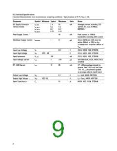
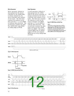
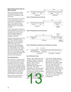
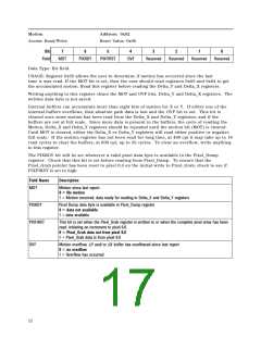
Required timing between Read and
Write Commands
tSWW
SCLK
There are minimum timing
requirements between read
and write commands on the
serial port.
Address
Write Operation
Data
Address
Data
Write Operation
Figure 17. Timing between two write commands
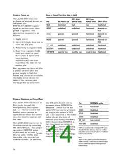
If the rising edge of the SCLK
for the last data bit of the
second write command occurs
before the required delay
tSWR
SCLK
Address
Write Operation
Data
Address
(t
), then the first write
SWW
command may not complete
correctly.
Next Read
Operation
If the rising edge of SCLK for
the last address bit of the read
command occurs before the
Figure 18. Timing between write and read commands
required delay (t
write command may not
complete correctly.
), the
SWR
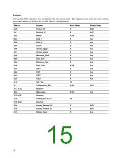
tSRW & tSRR
tSRAD
SCLK
During a read operation SCLK
should be delayed at least
Address
Data
Address
Read Operation
Next Read or
t
after the last address
Write Operation
SRAD
data bit to ensure that the
ADNS-3040 has time to
prepare the requested data.
The falling edge of SCLK for
the first address bit of either
the read or write command
Figure 19. Timing between read and either write or subsequent read commands
t
SRAD
SCLK
must be at least t
or t
SRR
SRW
Motion_Burst Register Address
Read First Byte
after the last SCLK rising edge
of the last data bit of the
previous read operation.
First Read Operation
Read Second Byte
Read Third Byte
Figure 20. Motion Burst Timing
Burst Mode Operation
read with no delay between
bytes by driving SCLK at the
normal rate. The data is
latched into the output buffer
after the last address bit is
received. After the burst
register. The ADNS-3040 will
respond with the contents of
the Motion, Delta_Y, Delta_X,
SQUAL, Shutter_Upper,
Shutter_Lower and
Maximum_Pixel registers in
that order. The burst
transaction can be terminated
after the first 3 bytes of the
sequence are read by bringing
the NCS pin high. After
sending the register address,
the micro-controller must wait
Burst mode is a special serial
port operation mode that may
be used to reduce the serial
transaction time for a motion
read. The speed improvement
is achieved by continuous data
clocking from multiple registers
without the need to specify the
register address, and by not
requiring the normal delay
transmission is complete, the
micro-controller must raise the
NCS line for at least t
to
BEXIT
terminate burst mode. The
serial port is not available for
use until it is reset with NCS,
even for a second burst
transmission.
period between data bytes.
Burst mode is activated by
reading the Motion_Burst
t
and then begin reading
SRAD
data. All data bits can be
13

 AGILENT [ AGILENT TECHNOLOGIES, LTD. ]