Data Sheet
July 2000
LU6612
FASTCAT Single-FET for 10Base-T/100Base-TX
MII Station Management (continued)
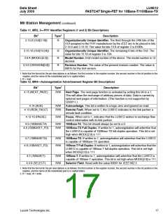
Table 18. MR29—Device-Specific Register 2 (100 Mbits/s Control) Bit Descriptions
Bit1
Type2
Description
29.15 (LOCALRST)
R/W Management Reset. This is the local management reset bit. Writing a logic 1 to
this bit will cause the lower 16 registers and registers 28 and 29 to be reset to
their default values. This bit is self-clearing. The default is 0.
29.14 (RST1)
29.13 (RST2)
29.12 (100OFF)
R/W Generic Reset 1. This register is used for manufacture test only. The default is 0.
R/W Generic Reset 2. This register is used for manufacture test only. The default is 0.
R/W 100 Mbits/s Transmitter Off. When this bit is set to 0, it forces RX low and RY
high. This bit defaults to 1.
29.11
R/W Reserved. Program to zero.
29.10 (CRS_SEL)
R/W Carrier Sense Select. CRS will be asserted on receive only when this bit is set to
a 1. If this bit is set to logic 0, CRS will be asserted on receive or transmit. The
default is 0.
29.9 (LINK_ERR)
29.8 (PKT_ERR)
R/W Link Error Indication. When this bit is a 1, a link error code will be reported on
RXD[3:0] of the LU6612 when RX_ER is asserted on the MII. The specific error
codes are listed in the RXD pin description. If it is 0, it will disable this function.
The default is 0.
R/W Packet Error Indication Enable. When this bit is a 1, a packet error code, which
indicates that the scrambler is not locked, will be reported on RXD[3:0] of the
LU6612 when RX_ER is asserted on the MII. When this bit is 0, it will disable this
function. The default is 0.
29.7 (RESERVED)
29.6 (EDB)
R/W Reserved. This bit must remain as a zero. The default is 0.
R/W Encoder/Decoder Bypass. When this bit is set to 1, the 4B/5B encoder and
5B/4B decoder function will be disabled. The default is a zero. At powerup/reset, if
PCSEN is strapped low, then this bit is set to a 1. The default is 0.
29.5 (SAB)
29.4 (SDB)
R/W Symbol Aligner Bypass. When this bit is set to 1, the aligner function will be dis-
abled. The default is 0.
R/W Scrambler/Descrambler Bypass. When this bit is set to 1, the scrambling/
descrambling functions will be disabled. The default is a zero. At powerup/reset, if
PCSEN is strapped low, then this bit is set to a 1. The default is 0.
29.3 (CARIN_EN)
29.2 (JAM_COL)
R/W Carrier Integrity Enable. When this bit is set to a 1, carrier integrity is enabled.
(This function is not supported by QS6611.) The default is 0.
R/W Jam Enable. When this bit is a 1, it enables JAM associated with carrier integrity
to be ORed with COL. The default is 0.
29.1 (RESERVED)
29.0 (RESERVED)
R/W Reserved. This bit must remain as a zero. The default is 0.
R/W Reserved. This bit must remain as a zero. The default is 0.
1. Note that the format for the pin descriptions is as follows: the first number is the register number, the second number is the bit position in the
register, and the name of the instantiated pad is in capital letters.
2. R = read, W = write.
Lucent Technologies Inc.
21

 AGERE [ AGERE SYSTEMS ]