AD5940
Data Sheet
TABLE OF CONTENTS
Features .............................................................................................. 1
Avoiding Incoherency Errors Between Excitation and
Measurement Frequencies During Impedance Measurements
....................................................................................................... 41
Applications....................................................................................... 1
Simplified Block Diagram ............................................................... 1
Revision History ............................................................................... 3
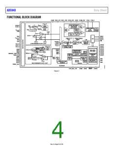
Functional Block Diagram .............................................................. 4
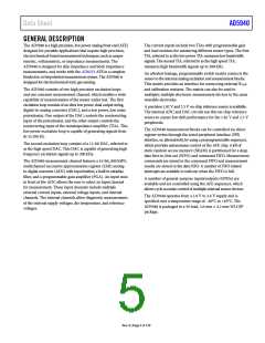
General Description......................................................................... 5
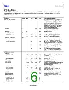
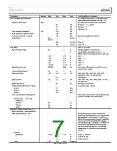
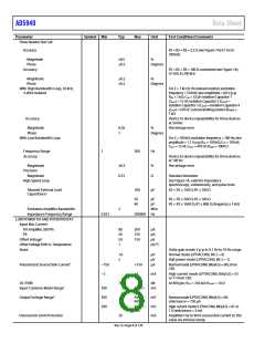
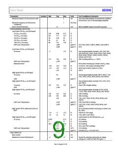
Specifications..................................................................................... 6
ADC RMS Noise Specifications ............................................... 15
SPI Timing Specifications ......................................................... 15
Absolute Maximum Ratings.......................................................... 17
Thermal Resistance .................................................................... 17
ESD Caution................................................................................ 17
Pin Configuration and Function Descriptions........................... 18
Typical Performance Characteristics ........................................... 20
Reference Test Circuit................................................................ 22
Theory of Operation ...................................................................... 23
Configuration Registers............................................................. 23
Silicon Identification...................................................................... 26
Identification Registers.............................................................. 26
Low Power DAC ............................................................................. 27
Low Power DAC Switch Options ............................................. 27
Relationship Between the 12-Bit and 6-Bit Outputs.............. 29
Low Power DAC Use Cases....................................................... 29
Low Power DAC Circuit Registers........................................... 30
Low Power Potentiostat ................................................................. 33
Low Power TIA ............................................................................... 34
Low Power TIA Protection Diodes .......................................... 34
Using an External RTIA ............................................................... 34
High Speed DAC Calibration Options.................................... 42
High Speed DAC Circuit Registers.......................................... 43
High Speed TIA Circuits ............................................................... 46
High Speed TIA Configuration................................................ 46
High Speed TIA Circuit Registers............................................ 48
High Performance ADC Circuit................................................... 50
ADC Circuit Overview.............................................................. 50
ADC Circuit Diagram ............................................................... 50
ADC Circuit Features ................................................................ 51
ADC Circuit Operation............................................................. 51
ADC Transfer Function............................................................. 51
ADC Low Power Current Input Channel ............................... 52
Selecting Inputs to ADC Mux .................................................. 52
ADC Postprocessing .................................................................. 52
Internal Temperature Sensor Channel .................................... 53
Sinc2 Filter (50 Hz/60 Hz Mains Filter).................................. 53
ADC Calibration ........................................................................ 53
ADC Circuit Registers............................................................... 54
ADC Calibration Registers ....................................................... 59
ADC Digital Postprocessing Registers (Optional) ................ 65
ADC Statistics Registers............................................................ 66
Programmable Switch Matrix....................................................... 68
Switch Descriptions ................................................................... 68
Recommended Configuration in Hibernate Mode ............... 68
Options for Controlling All Switches ...................................... 68
Programmable Switches Registers ........................................... 71
Precision Voltage References ........................................................ 81
Recommended Switch Settings for Various Operating
Modes........................................................................................... 34
High Power and Low Power Buffer Control Register—
BUFSENCON ............................................................................. 81
Low Power TIA Circuits Registers ........................................... 37
High Speed DAC Circuits.............................................................. 40
High Speed DAC Output Signal Generation.......................... 40
Power Modes of the High Speed DAC Core........................... 40
High Speed DAC Filter Options............................................... 40
High Speed DAC Output Attenuation Options ..................... 41
High Speed DAC Excitation Amplifier ................................... 41
Sequencer ........................................................................................ 83
Sequencer Features..................................................................... 83
Sequencer Overview .................................................................. 83
Sequencer Commands............................................................... 83
Sequencer Operation ................................................................. 85
Sequencer and FIFO Registers ................................................. 87
Waveform Generator...................................................................... 92
Waveform Generator Features.................................................. 92
Waveform Generator Operation .............................................. 92
Coupling an AC Signal from the High Speed DAC to the DC
Level Set by the Low Power DAC............................................. 41
Rev. 0 | Page 2 of 130

 ADI [ ADI ]