ADSemiconductor®
ANMG04 (4-CH Auto Sensitivity Calibration Capacitive Touch Sensor)
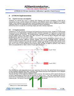
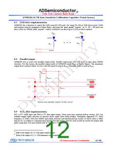
8.3 LED drive implementation
ANMG04 has a function to control the LED using D1~D4 ports. For using D1~D4 as LED driver ports, LEDs
and resisters must be equipped as below figure, and write the ‘port_mode” register5 as ‘1’. D1 ~ D4 ports can
drive LEDs by ‘PWM_ctrlx’ register6 control. ANMG04 can drive up to 8 LED as below method.
VDD
VDD
LED4
LED1
RD4
RD1
D1 <<
D4 <<
8.4 Parallel output
ANMG04 acts as active low parallel output mode. Parallel output ports (D1~D4) have an open drain NMOS
structure. For this reason, the parallel output mode of ANMG04 needs ROUT as below figures. The maximum
output drive current is 8mA, so over a few kΩ must be used as ROUT. Normally 10kΩ is used as ROUT
.
VDD
ROUT1
ROUT2
OUTPUT1
OUTPUT2
D1
D2
ROUT4
OUTPUT4
D4
Active low parallel output mode circuit
8.5 SCL, SDA implementation
SCL is I2C clock input and SDA is I2C data input-output. These ports have internal pull-up resistor. SCL has
Schmitt trigger input structure to prevent clock signal from being broken. Maximum supported I2C clock
frequency is 2MHz. SDA has NMOS open drain structure and internal pull-up resister of which value is 30kΩ
typical. So, according to communication speed a few kΩ resister must be used as pull-up resister for proper data
pulse rising time. For more details refer to ‘Chapter 9. I2C Interface’.
5
Refer to the chapter 10.2.12. Port mode control register
6
Refer to the chapter 10.2.11. LED luminance control register
AD Semiconductor Confidential
12 / 29

 ADI [ ADI ]