ADSemiconductor®
ANMG04 (4-CH Auto Sensitivity Calibration Capacitive Touch Sensor)
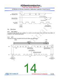
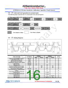
9.8 I2C write and read operations in normal mode
The following figure represents the I2C normal mode write and read registers.
☞ Write register 0x00 to 0x01 with data AA and BB
Device
Address 0x48
Register
Address 0x00
Start
ACK
ACK
Data AA
ACK
Data BB
ACK
Stop
Read register 0x00 and 0x01
Device
Address 0x48
Register
Address 0x00
Start
ACK
ACK
ACK
Stop
Device
Address 0x49
Start
ACK
Data Read AA
Data Read BB
Stop
ACK
From Slave to Master
From Master to Slave
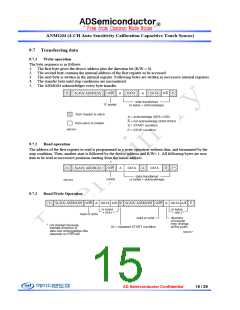
9.9 I2C timing diagram
100kbps
400kbps
PARAMETER
SYMBOL
UNIT
MIN.
4.0
4.7
4.0
4.7
1.0
250
-
MAX.
MIN.
MAX.
Hold time (repeated)START condition.
LOW period of the SCL clock
HIGH period of the SCL clock
Set-up time for a repeated START condition
Data hold time
tHD;STA
-
0.6
1.3
0.6
0.6
-
-
us
us
us
us
us
ns
ns
ns
us
tLOW
tHIGH
tSU;STA
tHD;DAT
tSU;DAT
tr
-
-
-
-
-
-
-
-
-
Data set-up time
100
20
-
Rise time of both SDA and SCL signals
Fall time of both SDA and SCL signals
Set-up time for STOP condition
1000
300
-
300
300
-
tf
-
20
tSU;STO
4.0
0.6
Bus free time between a STOP and START
condition
Noise margin at the LOW level for each
connected device
Noise margin at the HIGH level for each
connected device
tBUF
VnL
VnH
4.7
-
-
-
1.3
-
-
-
us
V
V
0.1VDD
0.2VDD
0.1VDD
0.2VDD
Input Low level
Input High level
0
VDD*0.2
VDD
V
V
VDD*0.8
AD Semiconductor Confidential
16 / 29

 ADI [ ADI ]