ADSemiconductor®
ANMG04 (4-CH Auto Sensitivity Calibration Capacitive Touch Sensor)
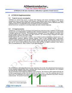
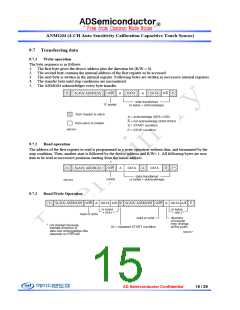
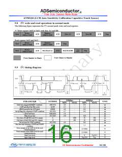
9.7 Transferring data
9.7.1
Write operation
The byte sequence is as follows:
1. The first byte gives the device address plus the direction bit (R/W = 0).
2. The second byte contains the internal address of the first register to be accessed.
3. The next byte is written in the internal register. Following bytes are written in successive internal registers.
4. The transfer lasts until stop conditions are encountered.
5. The ANMG04 acknowledges every byte transfer.
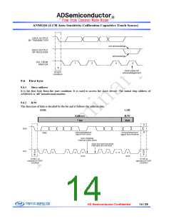
9.7.2
Read operation
The address of the first register to read is programmed in a write operation without data, and terminated by the
stop condition. Then, another start is followed by the device address and R/W= 1. All following bytes are now
data to be read at successive positions starting from the initial address.
9.7.3
Read/Write Operation
AD Semiconductor Confidential
15 / 29

 ADI [ ADI ]