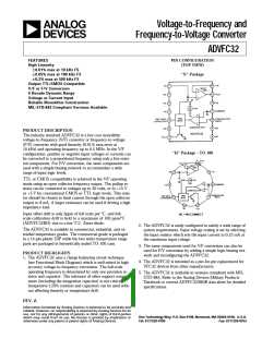
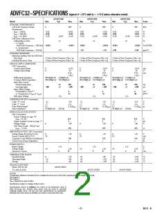
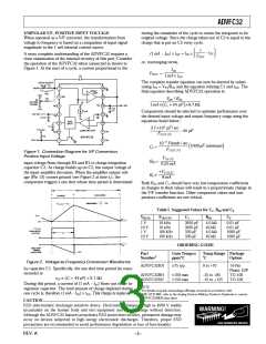
ADVFC32
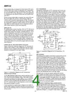
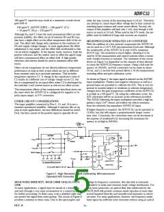
Figure 6. High Noise Im m unity Data Link
fiber link, and the optocoupler provides common-mode isolation
up to 3000 V dc.
Although the F/V conversion technique used in this circuit is
quite simple, it is also very limited in terms of its frequency re-
sponse and output ripple. T he frequency response is limited by
the integrator time constant and while it is possible to decrease
that time constant, either signal range or output ripple must be
sacrificed. T he performance of the circuit of Figure 6 is shown
in the photograph below. T he top trace is the input signal, the
middle trace is the frequency-modulated signal at the
T he data link input voltage is changed in a frequency modulated
signal by the first ADVFC32. A 42.2 kΩ input resistor and a
100 kΩ offset resistor set the scaling so that a 0 V input signal
corresponds to 50 kHz, and a 10 V input results in the maxi-
mum output frequency of 500 kHz. A high frequency opto-
coupler is then used to transmit the signal across any common-
mode voltage potentials to the receiving ADVFC32. T he opto-
coupler is not necessary in systems where common-mode noise
is either very small or a constant low level dc voltage. In systems
where common-mode voltage may present a problem, the con-
nection between the two locations should be through the opto-
coupler; no power or ground connections need to be made.
optocoupler’s output, and the bottom trace is the recovered
signal at the output of the F/V converter.
T he output of the optocoupler drives an ADVFC32 hooked up
in the F/V configuration. Since the reconstructed signal at Pin
10 has a considerable amount of carrier feedthrough, it is desir-
able to filter out any frequencies in the carrier range of 50 kHz
to 500 kHz. T he frequency response of the F/V converter is only
3 kHz due to the pole made by the integrator, so a second 3 kHz
filter will not significantly limit the bandwidth. With the simple
one pole filter shown in Figure 6, the input to output 3 dB point
is approximately 2 kHz, and the output noise is less than
15 mV. If a lower output impedance drive is needed, a two pole
active filter is recommended as an output stage.
O UTLINE D IMENSIO NS
D imensions shown in inches and (mm).
14-P in P lastic D IP P ackage
TO -100 P ackage
REV. A
–6–

 ADI [ ADI ]