ADVFC32
UNIP O LAR V/F, P O SITIVE INP UT VO LTAGE
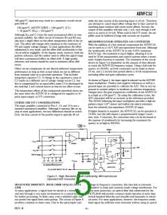
When operated as a V/F converter, the transformation from
voltage to frequency is based on a comparison of input signal
magnitude to the 1 mA internal current source.
during the remainder of the cycle to return the integrator to its
original voltage. Since the charge taken out of C2 is equal to the
charge that is put on C2 every cycle,
1
– tOS
(1 mA – IIN) × tOS = IIN
×
A more complete understanding of the ADVFC32 requires a
close examination of the internal circuitry of this part. Consider
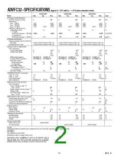
the operation of the ADVFC32 when connected as shown in
Figure 1. At the start of a cycle, a current proportional to the
F OUT
or, rearranging terms,
IIN
FOUT
=
1 mA × tOS
T he complete transfer equation can now be derived by substi-
tuting IIN = VIN/RIN and the equation relating C1 and tOS. T he
final equation describing ADVFC32 operation is:
VINI / RIN
1mA × C + 44 pF × 6.7 kΩ
(
)
1
Components should be selected to optimize performance over
the desired input voltage and output frequency range using the
equations listed below:
3.7 ×10⁷ pF / sec
– 44 pF
FOUT FS
10–4 Farads / sec
1000 pF minimum
(
)
C2 =
F OUT FS
Figure 1. Connection Diagram for V/F Conversion,
Positive Input Voltage
VIN FS
RIN
=
input voltage flows through R3 and R1 to charge integration
capacitor C2. As charge builds up on C2, the output voltage of
the input amplifier decreases. When the amplifier output volt-
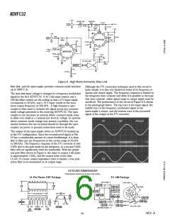
age (Pin 13) crosses ground (see Figure 2 at time t1), the
comparator triggers a one shot whose time period is determined
0.25 mA
+VLOGIC
8 mA
R2 ≥
Both RIN and C1 should have very low temperature coefficients
as changes in their values will result in a proportionate change in
the V/F transfer function. Other component values and tem-
perature coefficients are not critical.
Table I. Suggested Values for C 1, RIN and C2
VIN FS
FO UT FS
C1
RIN
C2
1 V
10 V
1 V
10 kHz
10 kHz
100 kHz
100 kHz
3650 pF
3650 pF
330 pF
330 pF
4.0 kΩ
40 kΩ
4.0 kΩ
40 kΩ
0.01 µF
0.01 µF
1000 pF
1000 pF
10 V
O RD ERING GUID E
Gain Tem pco Tem p Range P ackage
P art
Num ber 1
ppm /؇C
؇C
O ption
Figure 2. Voltage-to-Frequency Conversion Waveform s
ADVFC32KN
±75 typ
0 to +70
14-Pin
by capacitor C1. Specifically, the one shot time period (in nano-
seconds) is:
Plastic DIP
T O-100
T O-100
ADVFC32BH
ADVFC32SH
±100 max
±150 max
–25 to +85
–55 to +125
tOS (Cl + 44 pF) × 6.7 kΩ
During this period, a current of (1 mA – IIN) flows out of the in-
tegration capacitor. T he total amount of charge depleted during
one cycle is, therefore (1 mA – IIN) × tOS. This charge is replaced
NOT E
1For details on grade and package offerings screened in accordance with
MIL-ST D-883, refer to the Analog Devices Military Products Databook or current
ADVFC32/883B data sheet.
CAUTIO N
ESD (electrostatic discharge) sensitive device. Electrostatic charges as high as 4000 V readily
accumulate on the human body and test equipment and can discharge without detection.
Although the ADVFC32 features proprietary ESD protection circuitry, permanent damage may
occur on devices subjected to high energy electrostatic discharges. T herefore, proper ESD
precautions are recommended to avoid performance degradation or loss of functionality.
WARNING!
ESD SENSITIVE DEVICE
REV. A
–3–

 ADI [ ADI ]