ADVFC32–SPECIFICATIONS (typical @ +25؇C with V = ؎15 V unless otherwise noted)
S
AD VFC32K
Typ
AD VFC32B
Typ
AD VFC32S
Typ
Model
Min
Max
Min
Max
Min
Max
Units
DYNAMIC PERFORMANCE
Full Scale Frequency Range
Nonlinearity1
0
500
0
500
0
500
kHz
fMAX = 10 kHz
fMAX = 100 kHz
fMAX = 0.5 MHz
Full-Scale Calibration Error
(Adjustable to Zero)
vs. Supply
–0.01
–0.05
–0.20
±0.01
+0.05
+0.20
–0.01
–0.05
–0.20
+0.01
+0.05
+0.20
–0.01
–0.05
–0.20
+0.01
+0.05
+0.20
%
%
%
±0.05
±5
±0.05
±5
±0.05
±5
%
(Full Scale Frequency = 100 kHz) –0.015
vs. T emperature
(Full Scale Frequency = 10 kHz)
+0.015
–0.015
+0.015
–0.015
+150
+0.015
+150
% of FSR%
ppm/°C
±75
–100
+100
DYNAMIC RESPONSE
Maximum Settling T ime for Full Scale
Step Input
Overload Recovery T ime
1 Pulse of New Frequency Plus 1 µs
1 Pulse of New Frequency Plus 1 µs
1 Pulse of New Frequency Plus 1 µs
1 Pulse of New Frequency Plus 1 µs
1 Pulse of New Frequency Plus 1 µs
1 Pulse of New Frequency Plus 1 µs
ANALOG INPUT AMPLIFIER
(V/F Conversion)
Current Input Range
Voltage Input Range
0
0
+0.25
–10
0
0
+0.25
–10
0
0
+0.25
–10
mA
V2
0.25
0.25
× RIN
0.25
× RIN
mA
3
3
3
× RIN
2 MΩ||10 pF
300 MΩ||3 pF 750 MΩ||3 pF
Differential Impedance
Common-Mode Impedance
Input Bias Current
300 kΩ||10 pF
300 kΩ||10 pF 2 MΩ||10 pF
300 MΩ||3 pF 750 MΩ||10 pF
300 kΩ||10 pF 2 MΩ||10 pF
300 MΩ||3 pF 750 MΩ||10 pF
Noninverting Input
Inverting Input
40
±8
250
+100
40
±8
250
+100
40
±8
250
+100
nA
nA
–100
–100
–100
Input Offset Voltage
(T rimmable to Zero)2, 3
4
4
4
mV
vs. T emperature (T MIN to TMAX
Safe Input Voltage
)
30
30
30
µV/°C
±VS
±VS
±VS
COMPARAT OR (F/V Conversion)
Logic “0” Level
–VS
+1
0.1
–0.6
+VS
0.15/fMAX
–VS
+1
0.1
–0.6
+VS
–VS
+1
–0.6
+VS
0.15/fMAX µs
V
V
Logic “1” Level
Pulse Width Range4
Input Impedance
0.15/fMAX 0.1
50 kΩ||10 pF
50 kΩ||10 pF
250 kΩ
50 kΩ||10 pF
250 kΩ
250 kΩ
OPEN COLLECT OR OUT PUT
(V/F Conversion)
Output Voltage in Logic “0”
ISINK = 8 mA
Output Leakage Current in Logic “1”
Voltage Range
0.4
1
+30
0.4
1
+30
0.4
1
+30
V
µA
V
0
0
0
Fall T imes (Load = 500 pF and
ISINK = 5 mA)
400
+10
400
+10
400
+10
ns
AMPLIFIER OUT PUT (F/V Conversion)
Voltage Range (0 mA≤IO≤7 mA)
Source Current (0≤VO≤7 V)
Capacitive Load (Without Oscillation)
Closed Loop Output Impedance
0
10
0
10
0
10
V
mA
pF
Ω
100
1
100
1
100
1
POWER SUPPLY
Rated Voltage
±15
±15
±15
V
Voltage Range
±9
±18
±9
±18
±9
±18
V
Quiescent Current
6
8
6
8
6
8
mA
T EMPERAT URE RANGE
Specified Range
Operating Range
Storage
0
–25
–25
+70
+85
+85
–25
–55
–65
+85
+125
+150
–55
–55
–65
+125
+125
+150
°C
°C
°C
PACKAGE OPT IONS
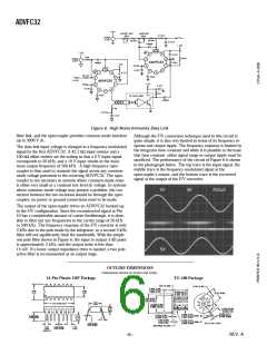
Plastic DIP (N-14)
T O–100 (H-10A)
ADVFC32KN
ADVFC32BH
ADVFC32SH
NOT ES
1Nonlinearity defined as deviation from a straight line from zero to full scale, expressed as a percentage of full scale.
2See Figure 3.
3See Figure 1.
4fMAX expressed in units of MHz.
Specifications subject to change without notice.
Specifications shown in boldface are tested on all production units at
final electrical test. Results from those tests are used to calculate
outgoing quality levels. All min and max specifications are guaranteed,
although only those shown in boldface are tested on all production units.
–2–
REV. A

 ADI [ ADI ]