ADVFC32
F/V CO NVERSIO N
Input resistance RIN is composed of a fixed resistor (R1) and a
variable resistor (R3) to allow for initial gain error compensation.
T o cover all possible situations, R3 should be 20% of RIN, and
R1 should be 90% of RIN. T his allows a ±10% gain adjustment
to compensate for the ADVFC32 full-scale error and the toler-
ance of C1.
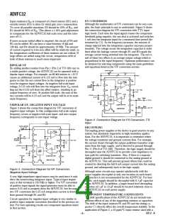
Although the mathematics of F/V conversion can be very com-
plex, the basic principle is easy to understand. Figure 4 shows
the connection diagram for F/V conversion with T T L input
logic levels. Each time the input signal crosses the comparator
threshold going negative, the one shot is activated and switches
1 mA into the integrator input for a measured time period (de-
termined by C1). As the frequency increases, the amount of
charge injected into the integration capacitor increases propor-
tionately. T he voltage across the integration capacitor is stabi-
lized when the leakage current through R1 and R3 equals the
average current being switched into the integrator. T he net re-
sult of these two effects is an average output voltage which is
proportional to the input frequency. Optimum performance can
be obtained by selecting components using the same guidelines
and equations listed in the V/F conversion section.
If more accurate initial offset is required, the circuit of R4 and
R5 can be added. R5 can have a value between 10 kΩ and
100 kΩ, and R4 should be approximately 10 MΩ. T he amount
of current required to trim zero offset will be relatively small, so
the temperature coefficients of these resistors are not critical. If
large offsets are added using this circuit, temperature drift of
both of these resistors is much more important.
BIP O LAR V/F
By adding another resistor from Pin 1 (Pin 2 of T O-100 can) to
a stable positive voltage, the ADVFC32 can be operated with a
bipolar input voltage. For example, an 80 kΩ resistor to +10 V
causes an additional current of 0.125 mA to flow into the inte-
grator so that the net current flow to the integrator is positive
even for negative input voltages. At negative full-scale input
voltage, 0.125 mA will flow into the integrator from VIN cancel-
ling out the 0.125 mA from the offset resistor, resulting in an
output frequency of zero. At positive full scale, the sum of the
two currents will be 0.25 mA and the output will be at its maxi-
mum frequency.
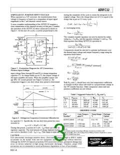
UNIP O LAR V/F, NEGATIVE INP UT VO LTAGE
Figure 3 shows the connection diagram for V/F conversion of
negative input voltages. In this configuration full-scale output
frequency occurs at negative full-scale input, and zero output
frequency corresponds to zero input voltage.
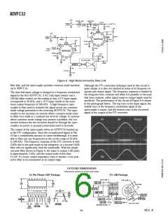
Figure 4. Connection Diagram for F/V Conversion, TTL
Input
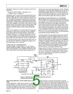
D ECO UP LING
Decoupling power supplies at the device is good practice in any
system, but absolutely imperative in high resolution applica-
tions. For the ADVFC32, it is important to remember where
the voltage transients and ground currents flow. For example,
the current drawn through the output pulldown transistor origi-
nates from the logic supply, and is directed to ground through
Pin 11 (Pin 8 of T O-100). T herefore, the logic supply should be
decoupled near the ADVFC32 to provide a low impedance re-
turn path for switching transients. Also, if there is a separate
digital ground it should be connected to the analog ground at
the ADVFC32. T his will prevent ground offsets that could be
created by directing the full 8 mA output current into the analog
ground, and subsequently back to the logic supply.
Figure 3. Connection Diagram for V/F Conversion,
Negative Input Voltage
Although some circuits may operate satisfactorily with the
power supplies decoupled at only one location on each board,
this practice is not recommended for the ADVFC32. For best
results, each supply should be decoupled with 0.1 µF capacitor
at the ADVFC32. In addition, a larger board level decoupling
capacitor of 1 µF to 10 µF should be located relatively close to
the ADVFC32 on each power supply.
A very high impedance signal source may be used since it only
drive the noninverting integrator input. T ypical input imped-
ance at this terminal is 250 MΩ or higher. For V/F conversion
of positive input signals the signal generator must be able to
source 0.25 mA to properly drive the ADVFC32, but for nega-
tive V/F conversion the 0.25 mA integration current is drawn
from ground through R1 and R3.
CO MP O NENT TEMP ERATURE CO EFFICIENTS
T he drift specifications of the ADVFC32 do not include tem-
perature effects of any of the supporting resistors or capacitors.
T he drift of the input resistors R1 and R3 and the timing ca-
pacitor C1 directly affect the overall temperature stability. In the
application of Figure 2, a 10 ppm/°C input resistor used with a
Circuit operation for negative input voltages is very similar to
positive input unipolar conversion described in the previous sec-
tion. For best operating results use component equations listed
in that section.
REV. A
–4–

 ADI [ ADI ]