ADM3485E
ABSOLUTE MAXIMUM RATINGS*
(TA = +25°C unless otherwise noted)
Operating Temperature Range
Industrial (A Version) . . . . . . . . . . . . . . . . –40°C to +85°C
Storage Temperature Range . . . . . . . . . . . . –65°C to +150°C
Lead Temperature (Soldering, 10 sec) . . . . . . . . . . . . +300°C
Vapor Phase (60 sec) . . . . . . . . . . . . . . . . . . . . . . . . +215°C
Infrared (15 sec) . . . . . . . . . . . . . . . . . . . . . . . . . . . +220°C
ESD Rating: Air (Human Body Model, All Pins) . . . . . >4 kV
ESD Rating: IEC1000-4-2 Contact (A, B Pins) . . . . . . >8 kV
EFT Rating: IEC1000-4-4 (A, B Pins) . . . . . . . . . . . . . >2 kV
VCC . . . . . . . . . . . . . . . . . . . . . . . . . . . . . . . . . . . . . . . . . +7 V
Inputs
Driver Input (DI) . . . . . . . . . . . . . . . . –0.3 V to VCC + 0.3 V
Control Inputs (DE, RE) . . . . . . . . . . –0.3 V to VCC + 0.3 V
Receiver Inputs (A, B) . . . . . . . . . . . . . . . –7.5 V to +12.5 V
Outputs
Driver Outputs . . . . . . . . . . . . . . . . . . . . . –7.5 V to +12.5 V
Receiver Output . . . . . . . . . . . . . . . . . –0.5 V to VCC + 0.5 V
Power Dissipation 8-Lead DIP . . . . . . . . . . . . . . . . . 800 mW
θJA, Thermal Impedance . . . . . . . . . . . . . . . . . . . . 140°C/W
Power Dissipation 8-Lead SOIC . . . . . . . . . . . . . . . . 650 mW
θJA, Thermal Impedance . . . . . . . . . . . . . . . . . . . . 115°C/W
*Stresses above those listed under Absolute Maximum Ratings may cause perma-
nent damage to the device. This is a stress rating only; functional operation of the
device at these or any other conditions above those listed in the operational sections
of this specification is not implied. Exposure to absolute maximum ratings for
extended periods of time may affect device reliability.
ORDERING GUIDE
Model
Temperature Range
Package Description
Package Options
ADM3485EAN
ADM3485EAR
–40°C to +85°C
–40°C to +85°C
Plastic DIP
Small Outline (SOIC)
N-8
SO-8
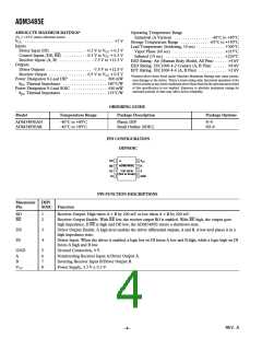
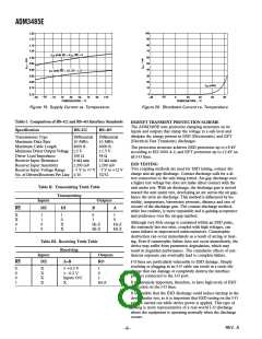
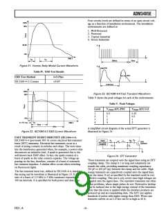
PIN CONFIGURATION
DIP/SOIC
1
2
3
4
8
7
6
5
RO
V
CC
ADM3485E
B
RE
DE
DI
TOP VIEW
(Not to Scale)
A
GND
PIN FUNCTION DESCRIPTIONS
Mnemonic
Pin
DIP/
SOIC Function
RO
RE
1
2
Receiver Output. High when A > B by 200 mV or low when A < B by 200 mV.
Receiver Output Enable. With RE low, the receiver output RO is enabled. With RE high, the output goes
high impedance. If RE is high and DE low, the ADM3485E enters a shutdown state.
DE
DI
3
4
Driver Output Enable. A high level enables the driver differential outputs, A and B. A low level places it in a
high impedance state.
Driver Input. When the driver is enabled, a logic low on DI forces A low and B high, while a logic high on DI
forces A high and B low.
GND
A
B
5
6
7
8
Ground Connection, 0 V.
Noninverting Receiver Input A/Driver Output A.
Inverting Receiver Input B/Driver Output B.
Power Supply, 3.3 V 0.3 V.
VCC
REV. A
–4–

 ADI [ ADI ]