(V = +3.3 V ꢁ 0.3 V. All specifications TMIN to TMAX unless otherwise noted.)
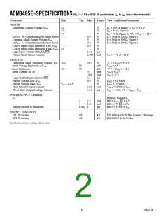
ADM3485E–SPECIFICATIONS
CC
Parameter
Min
Typ Max
Units Test Conditions/Comments
DRIVER
Differential Output Voltage, VOD
2.0
1.5
1.5
V
V
V
V
V
V
V
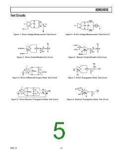
RL = 100 Ω, Figure 1, VCC > 3.1 V
RL = 54 Ω, Figure 1
RL = 60 Ω, Figure 2, –7 V < VTST < +12 V
R = 54 Ω or 100 Ω, Figure 1
R = 54 Ω or 100 Ω, Figure 1
R = 54 Ω or 100 Ω, Figure 1
∆|VOD| for Complementary Output States
Common-Mode Output Voltage VOC
∆|VOC| for Complementary Output States
CMOS Input Logic Threshold Low, VINL
0.2
3
0.2
0.8
CMOS Input Logic Threshold High, VINH 2.0
Logic Input Current (DE, DI, RE)
Output Short Circuit Current
V
µA
mA
1.0
250
VO = –7 V or +12 V
RECEIVER
Differential Input Threshold Voltage, VTH –0.2
+0.2
V
–7 V < VCM < +12 V
VCM = 0 V
–7 V < VCM < +12 V
VIN = +12 V
Input Voltage Hysteresis, ∆VTH
Input Resistance
50
19
+1
–0.8
1
mV
kΩ
mA
mA
µA
V
12
Input Current (A, B)
VIN = –7 V
Logic Enable Input Current (RE)
Output Voltage Low, VOL
Output Voltage High, VOH
0.4
IOUT = +2.5 mA
IOUT = –1.5 mA
VCC – 0.4 V
V
Short Circuit Output Current
Three-State Output Leakage Current
60
1.0
mA
µA
VOUT = GND or VCC
VCC = 3.6 V, 0 V < VOUT < VCC
POWER SUPPLY CURRENT
ICC
Outputs Unloaded,
DE = VCC, RE = 0 V
DE = 0 V, RE = 0 V
DE = 0 V, RE = VCC
1
1
1.2
1.2
1
mA
mA
µA
Supply Current in Shutdown
0.002
ESD/EFT IMMUNITY
ESD Protection
EFT Protection
8
2
kV
kV
IEC1000-4-2 A, B Pins Contact Discharge
IEC1000-4-4, A, B Pins
Specifications subject to change without notice.
–2–
REV. A

 ADI [ ADI ]