Data Sheet
AD7904/AD7914/AD7924
Digital Inputs
from a 3 V supply. The AD7904/AD7914/AD7924 have better
dynamic performance with a VDD of 5 V while still being able to
interface to 3 V processors. Care should be taken to ensure that
The digital inputs applied to the AD7904/AD7914/AD7924 can
go to 7 V and are not restricted by the AVDD + 0.3 V limit on the
analog inputs.
V
DRIVE does not exceed AVDD by more than 0.3 V (see the
Absolute Maximum Ratings section).
CS
Because the SCLK, DIN, and
AVDD + 0.3 V limit, power supply sequencing issues are avoided.
inputs are not restricted by the
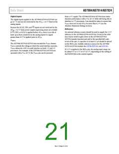
Reference
An external reference source should be used to supply the 2.5 V
reference to the AD7904/AD7914/AD7924. Errors in the refer-
ence source result in gain errors in the AD7904/AD7914/
AD7924 transfer function and add to the specified full-scale
errors of the part. A capacitor of at least 0.1 µF should be placed
on the REFIN pin. Suitable reference sources for the AD7904/
AD7914/AD7924 include the AD780, REF193, and AD1582.
CS
If , DIN, or SCLK is applied before AVDD, there is no risk of
latch-up as there would be on the analog inputs if a signal
greater than 0.3 V is applied prior to AVDD
.
VDRIVE
The AD7904/AD7914/AD7924 also include the VDRIVE feature.
DRIVE controls the voltage at which the serial interface operates.
DRIVE allows the ADC to easily interface to both 3 V and 5 V
processors. For example, if the AD7904/AD7914/AD7924 are
operated with a VDD of 5 V, the V DRIVE pin can be powered
V
V
If 2.5 V is applied to the REFIN pin, the analog input range can
be either 0 V to 2.5 V or 0 V to 5 V, depending on the setting of
the RANGE bit in the control register.
Rev. C | Page 21 of 32

 ADI [ ADI ]