Data Sheet
AD7904/AD7914/AD7924
POWER vs. THROUGHPUT RATE
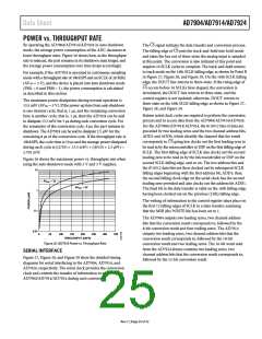
By operating the AD7904/AD7914/AD7924 in auto shutdown
mode, the average power consumption of the ADC decreases at
lower throughput rates. Figure 26 shows how, as the throughput
rate is reduced, the part remains in its shutdown state longer, and
the average power consumption over time drops accordingly.
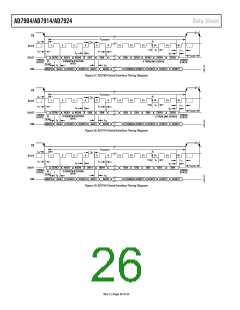
CS
signal initiates the data transfer and conversion process.
The
CS
The falling edge of
puts the track-and-hold into hold mode
and takes the bus out of three-state; the analog input is sampled
at this point. The conversion is also initiated at this point and
requires 16 SCLK cycles to complete. The track-and-hold returns
to track mode on the 14th SCLK falling edge, as shown by Point B
in Figure 27, Figure 28, and Figure 29. On the 16th SCLK falling
edge, the DOUT line returns to three-state. If the rising edge of
For example, if the AD7924 is operated in continuous sampling
mode with a throughput rate of 100 kSPS and an SCLK of 20 MHz
(AVDD = 5 V), and the device is placed into auto shutdown mode
(PM1 = 0 and PM0 = 1), the power consumption is calculated
as described in this section.
CS
occurs before 16 SCLKs have elapsed, the conversion is
terminated, the DOUT line returns to three-state, and the
control register is not updated; otherwise, DOUT returns to
three-state on the 16th SCLK falling edge, as shown in Figure 27,
Figure 28, and Figure 29.
The maximum power dissipation during normal operation is
13.5 mW (AVDD = 5 V). If the power-up time from auto shutdown
is one dummy cycle, that is, 1 µs, and the remaining conversion
time is another cycle, that is, 1 µs, then the AD7924 can be said
to dissipate 13.5 mW for 2 µs during each conversion cycle. For
the remainder of the conversion cycle, 8 µs, the part remains in
shutdown. The AD7924 can be said to dissipate 2.5 µW for the
remaining 8 μs of the conversion cycle. If the throughput rate is
100 kSPS, the cycle time is 10 µs and the average power dissipated
during each cycle is ((2/10) × 13.5 mW) + ((8/10) × 2.5 µW) =
2.702 mW.
Sixteen serial clock cycles are required to perform the conversion
process and to access data from the AD7904/AD7914/AD7924.
For the AD7904/AD7914/AD7924, the 8/10/12 bits of data are
preceded by two leading zeros and the two channel address bits,
ADD1 and ADD0, which identify the channel that the result
CS
corresponds to.
going low clocks out the first leading zero to
be read in by the microcontroller or DSP on the first falling edge of
SCLK. The first falling edge of SCLK also clocks out the second
leading zero to be read in by the microcontroller or DSP on the
second SCLK falling edge, and so on. The two address bits and
the 8/10/12 data bits are then clocked out by subsequent SCLK
falling edges beginning with the first address bit, ADD1; thus,
the second falling clock edge on the serial clock has the second
leading zero provided and also clocks out the address bit ADD1.
The final bit in the data transfer is valid on the 16th falling edge,
having been clocked out on the previous (15th) falling edge.
Figure 26 shows the maximum power vs. throughput rate when
using the auto shutdown mode with 5 V and 3 V supplies.
10
AV
= 5V
DD
AV
= 3V
DD
1
The writing of information to the control register takes place on
the first 12 falling edges of SCLK in a data transfer, assuming
that the MSB (the WRITE bit) has been set to 1.
0.1
The AD7904 outputs two leading zeros, two channel address
bits that the conversion result corresponds to, followed by the
8-bit conversion result and four trailing zeros. The AD7914
outputs two leading zeros, two channel address bits that the
conversion result corresponds to, followed by the 10-bit
conversion result and two trailing zeros. The 16-bit word read
from the AD7924 always contains two leading zeros, two
channel address bits that the conversion result corresponds to,
followed by the 12-bit conversion result.
0.01
0
50
100
150
200
250
300
350
THROUGHPUT (kSPS)
Figure 26. AD7924 Power vs. Throughput Rate
SERIAL INTERFACE
Figure 27, Figure 28, and Figure 29 show the detailed timing
diagrams for serial interfacing to the AD7904, AD7914, and
AD7924, respectively. The serial clock provides the conversion
clock and controls the transfer of information to and from the
AD7904/AD7914/AD7924 during each conversion.
Rev. C | Page 25 of 32

 ADI [ ADI ]