AD7904/AD7914/AD7924
Data Sheet
CIRCUIT INFORMATION
The AD7904/AD7914/AD7924 are, respectively, 8-bit, 10-bit,
and 12-bit, high speed, 4-channel, single-supply ADCs. The parts
can be operated from a 2.7 V to 5.25 V supply. When operated
from either a 5 V or 3 V supply, the AD7904/AD7914/AD7924
are capable of throughput rates of 1 MSPS when provided with
a 20 MHz clock.
condition. When the comparator is rebalanced, the conversion
is complete. The control logic generates the ADC output code.
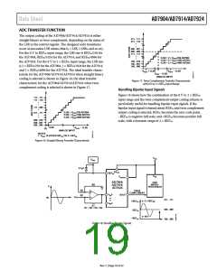
Figure 16 and Figure 17 show the ADC transfer functions.
CAPACITIVE
DAC
4kΩ
A
V
V
0
3
IN
CONTROL
LOGIC
SW1
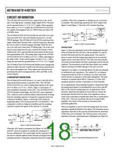
The AD7904/AD7914/AD7924 provide the user with an on-chip
track-and-hold ADC and serial interface housed in a 16-lead
TSSOP package. The AD7904/AD7914/AD7924 each have four
single-ended input channels with a channel sequencer, allowing
the user to select a channel sequence through which the ADC
B
SW2
IN
COMPARATOR
AGND
Figure 14. ADC Conversion Phase
CS
can cycle with each consecutive
falling edge. The serial clock
Analog Input
input accesses data from the part, controls the transfer of data
written to the ADC, and provides the clock source for the succes-
sive approximation ADC. The analog input range for the AD7904/
AD7914/AD7924 is 0 V to REFIN or 0 V to 2 × REFIN, depending on
the status of Bit 1 in the control register. For the 0 V to 2 × REFIN
range, the part must be operated from a 4.75 V to 5.25 V supply.
Figure 15 shows an equivalent circuit of the analog input structure
of the AD7904/AD7914/AD7924. The two diodes, D1 and D2,
provide ESD protection for the analog inputs. Care must be
taken to ensure that the analog input signal never exceeds the
supply rails by more than 200 mV. This will cause these diodes
to become forward-biased and start conducting current into the
substrate. The maximum current that these diodes can conduct
without causing irreversible damage to the part is 10 mA.
The AD7904/AD7914/AD7924 provide flexible power management
options to allow the user to achieve the best power performance
for a given throughput rate. These options are selected by pro-
gramming the power management bits, PM1 and PM0, in the
control register.
Capacitor C1 in Figure 15 is typically about 4 pF and can primarily
be attributed to pin capacitance. The resistor, R1, is a lumped
component made up of the on resistance of a track-and-hold
switch and the on resistance of the input multiplexer. The total
resistance is typically about 400 Ω. Capacitor C2 is the ADC
sampling capacitor and has a capacitance of 30 pF typically.
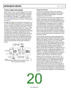
CONVERTER OPERATION
The AD7904/AD7914/AD7924 are 8-, 10-, and 12-bit SAR ADCs,
respectively, based around a capacitive DAC. The AD7904/
AD7914/AD7924 can convert analog input signals in the range
of 0 V to REFIN or 0 V to 2 × REFIN. Figure 13 and Figure 14
show simplified schematics of the ADC. The AD7904/AD7914/
AD7924 include control logic, the SAR ADC, and a capacitive
DAC, which are used to add and subtract fixed amounts of charge
from the sampling capacitor to bring the comparator back into
a balanced condition. Figure 13 shows the ADC during its
acquisition phase. SW2 is closed and SW1 is in Position A. The
comparator is held in a balanced condition and the sampling
capacitor acquires the signal on the selected VIN channel.
For ac applications, removing high frequency components from
the analog input signal is recommended by use of a low-pass RC
filter on the relevant analog input pin. In applications where
harmonic distortion and signal-to-noise ratio are critical, the
analog input should be driven from a low impedance source.
Large source impedances significantly affect the ac performance
of the ADC. This may necessitate the use of an input buffer
amplifier. The choice of the op amp is a function of the
particular application.
When no amplifier is used to drive the analog input, the source
impedance should be limited to low values. The maximum source
impedance depends on the amount of total harmonic distortion
(THD) that can be tolerated. The THD increases as the source
impedance increases, and performance will degrade (see Figure 8).
CAPACITIVE
DAC
4kΩ
A
V
V
0
3
IN
CONTROL
LOGIC
SW1
B
SW2
AV
DD
IN
COMPARATOR
AGND
C2
30pF
D1
Figure 13. ADC Acquisition Phase
R1
V
IN
When the ADC starts a conversion (see Figure 14), SW2 opens
and SW1 moves to position B, causing the comparator to
become unbalanced. The control logic and the capacitive DAC
are used to add and subtract fixed amounts of charge from the
sampling capacitor to bring the comparator back into a balanced
C1
4pF
D2
CONVERSION PHASE: SWITCH OPEN
TRACK PHASE: SWITCH CLOSED
Figure 15. Equivalent Analog Input Circuit
Rev. C | Page 18 of 32

 ADI [ ADI ]