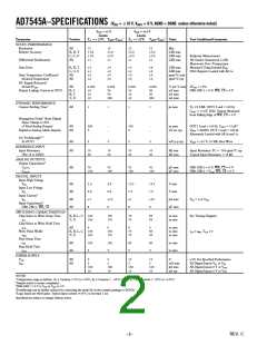
AD7545A
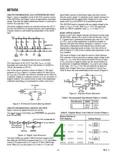
The circuits of Figures 4, 5 and 6 can all be converted to single
supply operation by biasing AGND to some voltage between
Figure 12 shows an alternative approach for use with 8-bit pro-
cessors which have a full 16-bit wide address bus such as 6800,
8080, Z80. This technique uses the 12 lower address lines of the
processor address bus to supply data to the DAC, thus each
AD7545A connected in this way uses 4k bytes of address loca-
tions. Data is written to the DAC using a single memory write
instruction. The address field of the instruction is organized so
that the lower 12 bits contain the data for the DAC and the
upper 4 bits contain the address of the 4k block at which the
DAC resides.
V
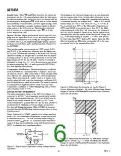
DD and DGND. Figure 10 shows the 2s Complement Bipolar
circuit of Figure 5 modified to give a range from +2 V to +8 V
about a “pseudo-analog ground” of 5 V. This voltage range
would allow operation from a single VDD of +10 V to +15 V.
The AD584 pin-programmable reference fixes AGND at +5 V.
VIN is set at +2 V by means of the series resistors R1 and R2.
There is no need to buffer the VREF input to the AD7545A with
an amplifier because the input impedance of the D/A converter
is constant. Note, however, that since the temperature coefficient
of the D/A reference input resistance is typically –300 ppm/°C,
applications which experience wide temperature variations may
require a buffer amplifier to generate the +2.0 V at the AD7545A
VREF pin. Other output voltage ranges can be obtained by changing
R4 to shift the zero point and (R1 + R2) to change the slope, or
gain of the D/A transfer function. VDD must be kept at least 5 V
above OUT1 to ensure that linearity is preserved.
Figure 12. Connecting the AD7545A to 8-Bit Processors
via the Address Bus
SUPPLEMENTAL APPLICATION MATERIAL
For further information on CMOS multiplying D/A converters
the reader is referred to the following texts:
Figure 10. Single Supply "Bipolar" 2s Complement D/A
Converter
Reference 1
CMOS DAC Application Guide available from Analog Devices,
Publication Number G872a-15-4/86.
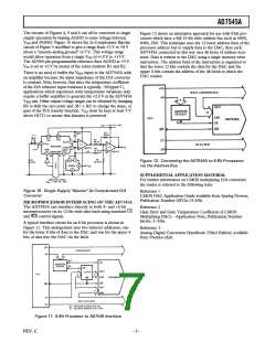
MICROPROCESSOR INTERFACING OF THE AD7545A
The AD7545A can interface directly to both 8- and 16-bit
microprocessors via its 12-bit wide data latch using standard CS
and WR control signals.
Reference 2
Gain Error and Gain Temperature Coefficient of CMOS
Multiplying DACs – Application Note, Publication Number
E630c–5–3/86.
A typical interface circuit for an 8-bit processor is shown in
Figure 11. This arrangement uses two memory addresses, one
for the lower 8 bits of data to the DAC and one for the upper 4
bits of data into the DAC via the latch.
Reference 3
Analog-Digital Conversion Handbook (Third Edition) available
from Prentice-Hall.
Figure 11. 8-Bit Processor to AD7545 Interface
REV. C
–7–

 ADI [ ADI ]