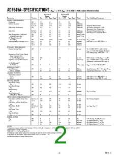
AD7545A–SPECIFICATIONS (VREF = ؎10 V, VOUT1 = O V, AGND = DGND unless otherwise noted)
VDD = +5 V
Limits
TA = + 25؇C TMIN–TMAX
VDD = +15 V
Limits
1
1
Parameter
Version
TA = + 25؇C
TMIN–TMAX
Units
Test Conditions/Comments
STATIC PERFORMANCE
Resolution
Relative Accuracy
All
12
1/2
1/2
1
12
1/2
1/2
1
12
1/2
1/2
1
12
1/2
1/2
1
Bits
K, B, T
L, C, U
All
LSB max
LSB max
LSB max
Endpoint Measurement
All Grades Guaranteed 12-Bit
Monotonic Over Temperature
Measured Using Internal RFB
DAC Register Loaded with All 1s.
Differential Nonlinearity
Gain Error
K, B, T
L, C, U
All
3
1
5
2
4
2
5
2
3
1
5
2
4
2
5
2
LSB max
LSB max
ppm/°C max
ppm/°C typ
.
Gain Temperature Coefficient2
∆Gain/∆Temperature
All
DC Supply Rejection2
∆Gain/∆VDD
All
0.002
10
10
0.004
50
50
0.002
10
10
0.004
50
50
% per % max ∆VDD
=
5%
Output Leakage Current at OUT1
K, L
B, C
T, U
nA max
nA max
nA max
DB0–DB11 = 0 V; WR, CS = 0 V
10
200
10
200
DYNAMIC PERFORMANCE
Current Settling Time2
All
1
1
1
1
µs max
To 1/2 LSB. OUT1 Load = 100 Ω,
CEXT = 13 pF. DAC Output Measured
from Falling Edge of WR, CS = 0 V.
Propagation Delay2 (from Digital
Input Change to 90%
of Final Analog Output)
All
All
200
5
–
–
150
5
–
–
ns max
nV sec typ
OUT1 Load = 100 Ω, CEXT = 13 pF3
VREF = AGND. OUT1 Load = 100 Ω,
Alternately Loaded with All 0s and 1s.
Digital-to-Analog Glitch Impulse
AC Feedthrough2, 4
At OUT1
All
All
5
5
5
5
mV p-p typ
VREF = 10 V, 10 kHz Sine Wave
REFERENCE INPUT
Input Resistance
10
20
10
20
10
20
10
20
kΩ min
kΩ max
Input Resistance TC = –300 ppm/°C typ
Typical Input Resistance = 15 kΩ
(Pin 19 to GND)
ANALOG OUTPUTS
Output Capacitance2
COUT1
All
70
150
70
150
70
150
70
150
pF max
pF max
DB0–DB11 = 0 V, WR, CS = 0 V
DB0–DB11 = VDD, WR, CS = 0 V
COUT1
DIGITAL INPUTS
Input High Voltage
VIH
All
All
All
All
2.4
0.8
1
2.4
0.8
10
8
13.5
1.5
1
13.5
1.5
10
V min
Input Low Voltage
VIL
V max
µA max
pF max
Input Current5
IIN
VIN = 0 or VDD
Input Capacitance2
DB0–DB11, WR, CS
8
8
8
SWITCHING CHARACTERISTICS2
Chip Select to Write Setup Time
tCS
K, B, L, C
T, U
100
100
130
170
75
75
85
95
ns min
ns min
See Timing Diagram
Chip Select to Write Hold Time
tCH
All
K, B, L, C
T, U
0
100
100
0
130
170
0
75
75
0
85
95
ns min
ns min
ns min
Write Pulse Width
tWR
tCS ≥ tWR, TCH ≥ 0
Data Setup Time
tDS
All
All
100
5
150
5
60
5
80
5
ns min
ns min
Data Hold Time
tDH
POWER SUPPLY
VDD
IDD
All
All
5
2
100
10
5
2
100
10
15
2
100
10
15
2
100
10
V
5% For Specified Performance
All Digital Inputs VIL or VIH
All Digital Inputs 0 V or VDD
All Digital Inputs 0 V or VDD
mA max
µA max
µA typ
NOTES
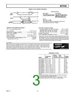
1Temperature range as follows: K, L Versions = 0°C to +70°C; B, C Versions = –25°C to +85°C; T, U Versions = –55°C to +125°C.
2Sample tested to ensure compliance.
3DB0–DB11 = 0 V to VDD or VDD to 0 V.
4Feedthrough can be further reduced by connecting the metal lid on the ceramic package to DGND.
6Logic inputs are MOS gates. Typical input current (+25°C) is less than 1 nA.
Specifications subject to change without notice.
–2–
REV. C

 ADI [ ADI ]