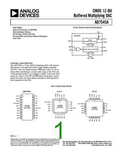
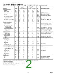
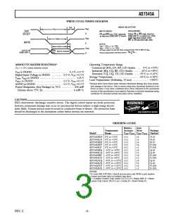
AD7545A
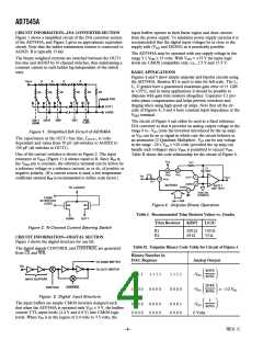
Invalid Data: When WR and CS are both low, the latches are
transparent and the D/A converter inputs follow the data inputs.
In some bus systems, data on the data bus is not always valid for
the whole period during which WR is low, and as a result invalid
data can briefly occur at the D/A converter inputs during a write
cycle. Such invalid data can cause unwanted signals or glitches
at the output of the D/A converter. The solution to this prob-
lem, if it occurs, is to retime the write pulse, WR, so it only
occurs when data is valid.
The loading on the reference voltage source is code-dependent
and the response time of the circuit is often determined by the
behavior of the reference voltage with changing load conditions.
To maintain linearity, the voltages at OUT1 and AGND should
remain within 2.5 volts of each other, for a VDD of 15 volts. If
VDD is reduced from 15 V, or the differential voltage between
OUT1 and AGND is increased to more than 2.5 V, the differ-
ential nonlinearity of the DAC will increase and the linearity of
the DAC will be degraded. Figures 8 and 9 show typical curves
illustrating this effect for various values of reference voltage and
VDD. If the output voltage is required to be offset from ground
by some value, then OUT1 and AGND may be biased up. The
effect on linearity and differential nonlinearity will be the same
as reducing VDD by the amount of the offset.
Digital Glitches: Digital glitches result due to capacitive cou-
pling from the digital lines to the OUT1 and AGND terminals.
This should be minimized by screening the analog pins of the
AD7545A (Pins 1, 2, 19, 20) from the digital pins by a ground
track run between Pins 2 and 3 and between Pins 18 and 19 of
the AD7545A.
Note how the analog pins are at one end (DIP) or side (LCC
and PLCC) of the package and separated from the digital pins
by VDD and DGND to aid screening at the board level. On-chip
capacitive coupling can also give rise to crosstalk from the digital-
to-analog sections of the AD7545A, particularly in circuits with
high currents and fast rise and fall times. This type of crosstalk is
minimized by using VDD = +5 volts. However, great care should
be taken to ensure that the +5 V used to power the AD7545A is
free from digitally induced noise.
Temperature Coefficients: The gain temperature coefficient
of the AD7545A has a maximum value of 5 ppm/°C and a typi-
cal value of 2 ppm/°C. This corresponds to worst case gain shifts
of 2 LSBs and 0.8 LSBs respectively over a 100°C temperature
range. When trim resistors R1 and R2 (such as in Figure 4) are
used to adjust full-scale range, the temperature coefficient of R1
and R2 should also be taken into account. The reader is referred
to Analog Devices Application Note “Gain Error and Gain
Temperature Coefficient to CMOS Multiplying DACs,” Publi-
cation Number E630c–5–3/86.
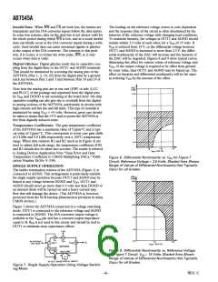
Figure 8. Differential Nonlinearity vs. VDD for Figure 7
Circuit. Reference Voltage = 2.5 Volts. Shaded Area Shows
Range of Values of Differential Nonlinearity that Typically
Occur for all Grades.
SINGLE SUPPLY OPERATION
The ladder termination resistor of the AD7545A (Figure 1) is
connected to AGND. This arrangement is particularly suitable
for single supply operation because OUT1 and AGND may be
biased at any voltage between DGND and VDD. OUT1 and
AGND should never go more than 0.3 volts less than DGND or
an internal diode will be turned on and a heavy current may
flow that will damage the device. (The AD7545A is, however,
protected from the SCR latchup phenomenon prevalent in many
CMOS devices.)
Figure 7 shows the AD7545A connected in a voltage switching
mode. OUT1 is connected to the reference voltage and AGND
is connected to DGND. The D/A converter output voltage is
available at the VREF pin and has a constant output impedance
equal to R. RFB is not used in this circuit and should be tied to
OUT1 to minimize stray capacitance effects.
Figure 9. Differential Nonlinearity vs. Reference Voltage
for Figure 7 Circuit. VDD = 15 Volts. Shaded Area Shows
Range of Values of Differential Nonlinearity that Typically
Occur for all Grades.
Figure 7. Single Supply Operation Using Voltage Switch-
ing Mode
–6–
REV. C

 ADI [ ADI ]