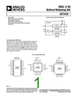
AD7545A
CIRCUIT INFORMATION—D/A CONVERTER SECTION
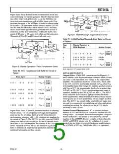
Figure 1 shows a simplified circuit of the D/A converter section
of the AD7545A, and Figure 2 gives an approximate equivalent
circuit. Note that the ladder termination resistor is connected to
AGND. R is typically 15 kΩ.
input buffers operate in their linear region and draw current
from the power supply. To minimize power supply currents it is
recommended that the digital input voltages be as close to the
supply rails (VDD and DGND) as is practically possible.
The AD7545A may be operated with any supply voltage in the
range 5 ≤ VDD ≤ 15 volts. With VDD = +15 V the input logic
levels are CMOS compatible only, i.e., 1.5 V and 13.5 V.
The binary weighted currents are switched between the OUT1
bus line and AGND by N-channel switches, thus maintaining a
constant current in each ladder leg independent of the switch
state.
BASIC APPLICATIONS
Figures 4 and 5 show simple unipolar and bipolar circuits using
the AD7545A. Resistor R1 is used to trim for full scale. The L,
C, U grades have a guaranteed maximum gain error of 1 LSB
at +25°C, and in many applications it should be possible to
dispense with gain trim resistors altogether. Capacitor C1 pro-
vides phase compensation and helps prevent overshoot and
ringing when using high speed op amps. Note that all the cir-
cuits of Figures 4, 5 and 6 have constant input impedance at the
VREF terminal.
The circuit of Figure 4 can either be used as a fixed reference
D/A converter so that it provides an analog output voltage in the
range 0 to –VIN (note the inversion introduced by the op amp)
or VIN can be an ac signal in which case the circuit behaves as
an attenuator (2-Quadrant Multiplier). VIN can be any voltage
in the range –20 ≤ VIN ≤ +20 volts (provided the op amp can
Figure 1. Simplified D/A Circuit of AD7545A
The capacitance at the OUT1 bus line, COUT1, is code-
dependent and varies from 70 pF (all switches to AGND) to
150 pF (all switches to OUT1).
handle such voltages) since VREF is permitted to exceed VDD
.
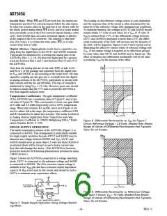
One of the current switches is shown in Figure 2. The input
resistance at VREF (Figure 1) is always equal to R. Since RIN at
the VREF pin is constant, the reference terminal can be driven by
a reference voltage or a reference current, ac or dc, of positive or
negative polarity. (If a current source is used, a low temperature
coefficient external RFB is recommended to define scale factor.)
Table II shows the code relationship for the circuit of Figure 4.
Figure 4. Unipolar Binary Operation
Table I. Recommended Trim Resistor Values vs. Grades
Trim Resistor
K/B/T
L/C/U
Figure 2. N-Channel Current Steering Switch
R1
R2
200 Ω
68 Ω
100 Ω
33 Ω
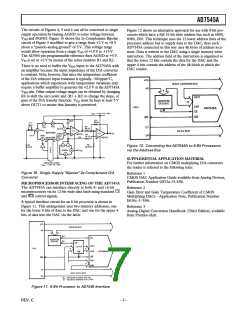
CIRCUIT INFORMATION—DIGITAL SECTION
Figure 3 shows the digital structure for one bit.
Table II. Unipolar Binary Code Table for Circuit of Figure 4
Binary Number in
The digital signals CONTROL and CONTROL are generated
from CS and WR.
DAC Register
Analog Output
4095
4096
1 1 1 1
1 1 1 1
1 1 1 1
–VIN
–VIN
–VIN
2048
4096
1 0 0 0
0 0 0 0
0 0 0 0
= –1/2 VIN
Figure 3. Digital Input Structure
1
4096
The input buffers are simple CMOS inverters designed such
that when the AD7545A is operated with VDD = 5 V, the buffers
convert TTL input levels (2.4 V and 0.8 V) into CMOS logic
levels. When VIN is in the region of 2.0 volts to 3.5 volts, the
0 0 0 0
0 0 0 0
0 0 0 0
0 0 0 0
0 0 0 1
0 0 0 0
0 Volts
–4–
REV. C

 ADI [ ADI ]