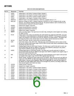
AD73360L
AD73360LA
Typ
Parameter
Min
Max
Unit
Test Conditions/Comments
LOGIC OUTPUT
VOH, Output High Voltage
VDD – 0.4
0
–10
VDD
0.4
+10
V
V
µA
|IOUT| ≤ 100 µA
|IOUT| ≤ 100 µA
V
OL, Output Low Voltage
Three-State Leakage Current
POWER SUPPLIES
AVDD1, AVDD2
DVDD
2.7
2.7
3.6
3.6
V
V
8
IDD
See Table I
NOTES
1Operating temperature range is as follows: –40°C to +85°C. Therefore, TMIN = –40°C and TMAX = +85°C.
2Test conditions: Input PGA set for 0 dB gain (unless otherwise noted).
3At input to sigma-delta modulator of ADC.
4Guaranteed by design.
5Overall group delay will be affected by the sample rate and the external digital filtering.
6The ADC’s input impedance is inversely proportional to DMCLK and is approximated by: (4 × 10¹¹)/DMCLK.
7Frequency response of ADC measured with input at audio reference level (the input level that produces an output level of –10 dBm0), with 38 dB preamplifier
bypassed and input gain of 0 dB.
8Test Conditions: no load on digital inputs, analog inputs ac-coupled to ground.
Specifications subject to change without notice.
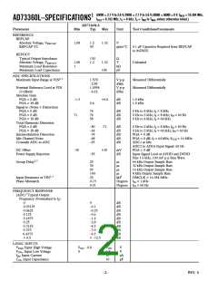
Table I. Current Summary (AVDD = DVDD = 3.3 V)
Total
Current
(Max)
MCLK
ON
Conditions
SE
Comments
ADCs Only On
25
1
0
0
1
0
0
Yes
No
No
Yes
Yes
No
REFOUT Disabled
REFOUT Disabled
REFCAP Only On
REFCAP and REFOUT Only On
All Sections On
All Sections Off
All Sections Off
1.0
3.5
26.5
1.0
0.05
REFOUT Enabled
MCLK Active Levels Equal to 0 V and DVDD
Digital Inputs Static and Equal to 0 V or DVDD
The above values are in mA and are typical values unless otherwise noted. MCLK = 16.384 MHz; SCLK = 16.384 MHz.
(AVDD = 2.7 V to 3.6 V; DVDD = 2.7 V to 3.6 V; AGND = DGND = 0 V; TA = TMlN to TMAX, unless other-
wise noted.)
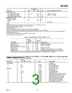
TIMING CHARACTERISTICS
Limit at
Parameter
TA = –40؇C to +85؇C
Unit
Description
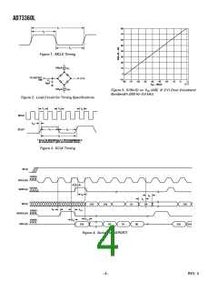
Clock Signals
See Figure 1.
t1
t2
t3
61
24.4
24.4
ns min
ns min
ns min
MCLK Period
MCLK Width High
MCLK Width Low
Serial Port
t4
t5
t6
t7
t8
t9
t10
t11
t12
t13
See Figures 3 and 4.
SCLK Period
SCLK Width High
SCLK Width Low
SDI/SDIFS Setup before SCLK Low
SDI/SDIFS Hold after SCLK Low
SDOFS Delay from SCLK High
SDOFS Hold after SCLK High
SDO Hold after SCLK High
SDO Delay from SCLK High
SCLK Delay from MCLK
t1
ns min
ns min
ns min
ns min
ns min
ns max
ns max
ns max
ns max
ns max
0.4 × t1
0.4 × t1
20
0
10
10
10
10
30
–3–
REV. 0

 ADI [ ADI ]