AD5290
Data Sheet
APPLICATIONS
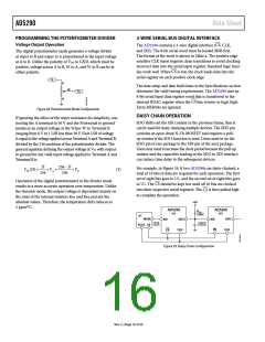
HIGH VOLTAGE DAC
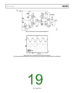
AUDIO VOLUME CONTROL
AD5290 can be configured as a high voltage DAC, with out-
put voltage as high as 30 V. The circuit is shown in Figure 33.
The output is
Because of its good THD performance and high voltage
capability, AD5290 can be used as a digital volume control.
If AD5290 is used directly as an audio attenuator or gain
amplifier, a large step change in the volume level at any arbi-
trary time can lead to an abrupt discontinuity of the audio
signal causing an audible zipper noise. To prevent this, a zero-
D
R
[1.2 V (1 2 )]
(4)
VO(D)
256
R1
CS
where D is the decimal code from 0 to 255.
crossing window detector can be inserted to the
line to
delay the device update until the audio signal crosses the
window. Since the input signal can operate on top of any
dc level rather than absolute zero volt level, zero-crossing in
this case means the signal is ac-coupled, and the dc offset
level is the signal zero reference point.
V
DD
V
DD
R
BIAS
U2
U1A
V+
OP284
V–
AD5290
D1
U1B
100kΩ
ADR512
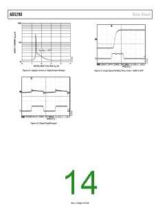
The configuration to reduce zipper noise (Figure 35) and the
results of using this configuration are shown in Figure 36. The
input is ac-coupled by C1 and attenuated down before feeding
into the window comparator formed by U2, U3, and U4B
(Figure 35). U6 is used to establish the signal zero reference.
The upper limit of the comparator is set above its offset and,
therefore, the output pulses high whenever the input falls
between 2.502 V and 2.497 V (or 0.005 V window) in this
example. This output is AND’ed with the chip select signal
such that the AD5290 updates whenever the signal crosses
the window. To avoid a constant update of the device, the
chip select signal should be programmed as two pulses, rather
than as one shown in Figure 36.
V
OUT
B
OP284
R2
R1
Figure 33. High Voltage DAC
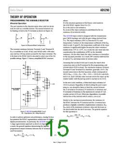
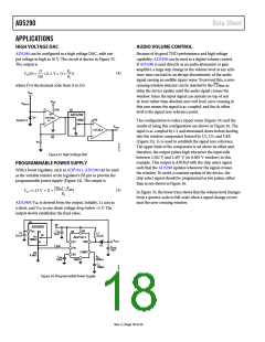
PROGRAMMABLE POWER SUPPLY
With a boost regulator, such as ADP1611, AD5290 can be used
as the variable resistor at the regulator’s FB pin to provide the
programmable power supply (Figure 34). The output is
D
(
256) RAB
R2
(5)
VO 1.23 V [1
]
In Figure 35, the lower trace shows that the volume level changes
from a quarter-scale to full-scale when a signal change occurs
near the zero-crossing window.
AD5290’s VDD is derived from the output. Initially, L1 acts as
a short, and VDD is one diode voltage drop below +5 V. The
output slowly establishes the final value.
U1
5V
AD5290
V
C
10F
IN
ADP1611
DD
IN
U2
A
C1
0.1F
L1
4.7H
W
R1
100k
V
OUT
SW
RT
B
D1
1.23V
C
C
OUT
10F
FB
SS
COMP
R2
8.5k
R
C
SS
GND
220k
22nF
C
C
150pF
Figure 34. Programmable Power Supply
Rev. C | Page 18 of 20

 ADI [ ADI ]