AD5290
Data Sheet
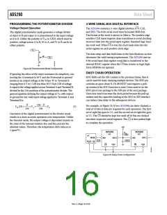
PROGRAMMING THE POTENTIOMETER DIVIDER
3-WIRE SERIAL BUS DIGITAL INTERFACE
Voltage Output Operation
CS
The AD5290 contains a 3-wire digital interface ( , CLK,
and SDI). The 8-bit serial word must be loaded MSB first.
The format of the word is shown in Table 4. The positive edge
sensitive CLK input requires clean transitions to avoid clocking
incorrect data into the serial input register. Standard logic fami-
The digital potentiometer easily generates a voltage divider
at wiper to B and wiper to A proportional to the input voltage
at A to B. Unlike the polarity of VDD to GND, which must be
positive, voltage across A to B, W to A, and W to B can be at
either polarity.
CS
lies work well. When
is low, the clock loads data into the
serial register on each positive clock edge.
V
I
A
The data setup and data hold times in the Specifications section
determine the valid timing requirements. The AD5290 uses an
8-bit serial input data register word that is transferred to the
W
V
O
B
CS
internal RDAC register when the
Extra MSB bits are ignored.
line returns to logic high.
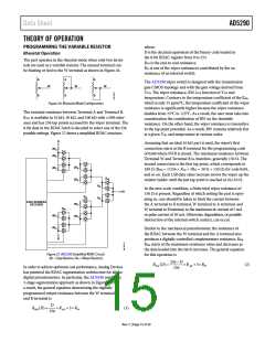
Figure 28. Potentiometer Mode Configuration
DAISY CHAIN OPERATION
If ignoring the effect of the wiper resistance for simplicity, con-
necting the A terminal to 30 V and the B terminal to ground
produces an output voltage at the Wiper W to Terminal B
ranging from 0 V to 1 LSB less than 30 V. Each LSB of voltage
is equal to the voltage applied across Terminal A and Terminal B,
divided by the 256 positions of the potentiometer divider. The
general equation defining the output voltage at VW with respect
to ground for any valid input voltage applied to Terminal A and
Terminal B is
SDO shifts out the SDI content in the previous frame; thus it
can be used for daisy-chaining multiple devices. The SDO pin
contains an open drain N-Ch MOSFET and requires a pull-
up resistor if the SDO function is used. Users need to tie the
SDO pin of one package to the SDI pin of the next package.
Users may need to increase the clock period because the pull-up
resistor and the capacitive loading at the SDO to SDI interface
can induce time delay to the subsequent devices.
D
256
256 − D
256
For example, in Figure 29, if two AD5290s are daisy-chained, a
total of 16 bits of data are required for each operation. The first
set of eight bits goes to U2, and the second set of eight bits goes
VW (D) =
×VA +
×VB
(3)
Operation of the digital potentiometer in the divider mode
results in a more accurate operation over temperature. Unlike
the rheostat mode, the output voltage is dependent mainly on
the ratio of the internal resistors RWA and RWB and not the
absolute values. Therefore, the temperature drift reduces to
5 ppm/°C.
CS
to U1. The
should be kept low until all 16 bits are clocked
into their respective serial registers. The
is then pulled high
CS
to complete the operation.
+5V
AD5290
AD5290
U2
R
PU
2.2kΩ
U1
µC
MOSI
SDO
SDI
SDO
CLK
SDI
SCLK SS
CS
CS
CLK
Figure 29. Daisy Chain Configuration
Rev. C | Page 16 of 20

 ADI [ ADI ]