Data Sheet
AD5290
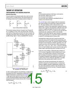
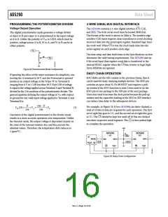
ESD PROTECTION
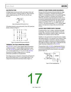
POWER-UP AND POWER-DOWN SEQUENCES
All digital inputs are protected with a series input resistor and
a Zener ESD structure, as shown in Figure 30. These structures
Because of the ESD protection diodes that limit the voltage
compliance at Terminal A, Terminal B, and Terminal W
(Figure 31), it is important to power VDD/VSS before applying
any voltage to Terminal A, Terminal B, and Terminal W.
Otherwise, the diodes are forward-biased such that VDD/VSS
are powered unintentionally and affect the system. Similarly,
VDD/VSS should be powered down last. The ideal power-up
sequence is as follows: GND, VDD, VSS, digital inputs, and
VA/VB/VW. The order of powering VA, VB, VW, and the digital
inputs is not important, as long as they are powered after
VDD/VSS.
CS
apply to digital input pins, Pin , Pin CLK, Pin SDI, and
Pin SDO.
340Ω
LOGIC
GND
Figure 30. Equivalent ESD Protection Circuit
All analog terminals are also protected by Zener ESD protection
diodes, as shown in Figure 31.
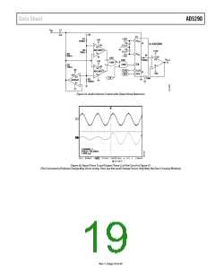
LAYOUT AND POWER SUPPLY BIASING
V
DD
It is good practice to use a compact, minimum lead-length
layout design. The leads to the input should be as direct as
possible, with a minimum conductor length. Ground paths
should have low resistance and low inductance.
A
W
B
Similarly, it is also good practice to bypass the power supplies
with quality capacitors. Low equivalent series resistance (ESR),
1 µF to 10 µF tantalum or electrolytic capacitors, should be
applied at the supplies to minimize any transient disturbance
and to filter low frequency ripple. Figure 32 illustrates the basic
supply-bypassing configuration for the AD5290.
V
SS
Figure 31. Equivalent ESD Protection Analog Pins
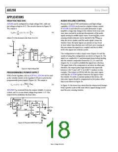
TERMINAL VOLTAGE OPERATING RANGE
The ground pin of the AD5290 is a digital ground reference.
To minimize the digital ground bounce, the AD5290 digital
ground terminal should be joined remotely to the analog
ground (Figure 32).
The AD5290 VDD and VSS power supplies define the boundary
conditions for proper 3-terminal digital potentiometer opera-
tion. The AD5290 can operate in single supply from +4.5 V to
+33 V or dual supply from 4.5 V to 16.5 V. T h e AD5290 is
functional at low supply voltages such as 4.5 V, but the
performance parameters are not guaranteed.
V
DD
V
DD
+
C1
C3
C4
10µF
0.1µF
0.1µF
AD5290
The voltages present on Terminal A, Terminal B, and Terminal W
that are more positive than VDD or more negative than VSS are
clamped by the internal forward-biased diodes (Figure 31).
+
C2
10µF
V
SS
V
SS
GND
Figure 32. Power Supply Bypassing
Rev. C | Page 17 of 20

 ADI [ ADI ]