AD5232
Data Sheet
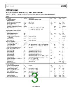
Parameter
DYNAMIC CHARACTERISTICS5, 9
Bandwidth
Total Harmonic Distortion
Symbol Conditions
−3 dB, BW_10kΩ, R = 10 kΩ
Min
Typ 1
Max
Unit
500
kHz
%
%
THDw
VA = 1 V rms, VB = 0 V, f = 1 kHz, RAB = 10 kΩ
VA = 1 V rms, VB = 0 V, f = 1 kHz, RAB = 50 kΩ, 100 kΩ
VDD = 5 V, VSS = 0 V, VA = VDD, VB = 0 V,
VW = 0.50% error band, Code 0x00 to Code 0x80
for RAB = 10 kΩ/50 kΩ/100 kΩ
0.022
0.045
0.65/3/6
VW Settling Time
tS
µs
Resistor Noise Voltage
Crosstalk (CW1/CW2)
eN_WB
CT
RWB = 5 kΩ, f= 1 kHz
VA = VDD, VB = 0 V, measure VW with
adjacent VR making full-scale code change
9
−5
nV/√Hz
nV-sec
Analog Crosstalk (CW1/CW2
)
CTA
VA1 = VDD, VB1 = 0 V, measure VW1 with VW2
=
−70
dB
5 V p-p @ f = 10 kHz; Code1 = 0x80; Code2 = 0xFF
FLASH/EE MEMORY RELIABILITY
Endurance10
Data Retention11
100
kCycles
Years
100
1 Typical parameters represent average readings at 25°C and VDD = 5 V.
2 Resistor position nonlinearity (R-INL) error is the deviation from an ideal value measured between the maximum resistance and the minimum resistance wiper
positions. R-DNL measures the relative step change from ideal between successive tap positions. Parts are guaranteed monotonic. IW ~ 50 µA @ VDD = 2.7 V and IW
400 µA @ VDD = 5 V for the RAB = 10 kΩ version, IW ~ 50 µA for the RAB = 50 kΩ version, and IW ~ 25 µA for the RAB = 100 kΩ version (see Figure 22).
~
3 INL and DNL are measured at VW with the RDACx configured as a potentiometer divider similar to a voltage output digital-to-analog converter. VA = VDD and VB = VSS
DNL specification limits of 1 LSB maximum are guaranteed monotonic operating conditions (see Figure 23).
4 The A, B, and W resistor terminals have no limitations on polarity with respect to each other. Dual supply operation enables ground-referenced bipolar signal
adjustment.
.
5 Guaranteed by design; not subject to production test.
6 Common-mode leakage current is a measure of the dc leakage from any A, B, or W terminal to a common-mode bias level of VDD/2.
7 Transfer (XFR) mode current is not continuous. Current is consumed while the EEMEMx locations are read and transferred to the RDACx register (see Figure 13).
8 PDISS is calculated from (IDD × VDD) + (ISS × VSS).
9 All dynamic characteristics use VDD = +2.5 V and VSS = −2.5 V, unless otherwise noted.
10 Endurance is qualified to 100,000 cycles per JEDEC Std. 22, Method A117 and measured at −40°C, +25°C, and +85°C. Typical endurance at +25°C is 700,000 cycles.
11
The retention lifetime equivalent at junction temperature (TJ) = 55°C, as per JEDEC Std. 22, Method A117. Retention lifetime, based on an activation energy of 0.6 eV,
derates with junction temperature as shown in Figure 44 in the Flash/EEMEM Reliability section. The AD5232 contains 9,646 transistors. Die size = 69 mil × 115 mil,
7,993 sq. mil.
Rev. C | Page 4 of 24

 ADI [ ADI ]