AD5232
Data Sheet
TABLE OF CONTENTS
Features .............................................................................................. 1
Digital Input/Output Configuration........................................ 14
Serial Data Interface................................................................... 15
Daisy-Chaining Operation........................................................ 15
Advanced Control Modes ......................................................... 17
Using Additional Internal, Nonvolatile EEMEM................... 18
Terminal Voltage Operating Range ......................................... 18
Detailed Potentiometer Operation .......................................... 18
Programming the Variable Resistor......................................... 19
Programming the Potentiometer Divider............................... 20
Operation from Dual Supplies ................................................. 20
Application Programming Examples ...................................... 20
Applications....................................................................................... 1
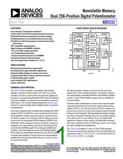
Functional Block Diagram .............................................................. 1
General Description ......................................................................... 1
Revision History ............................................................................... 2
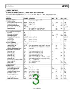
Specifications..................................................................................... 3
Electrical Characteristics—10 kΩ, 50 kΩ, 100 kΩ Versions .. 3
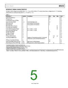
Interface Timing Characteristics................................................ 5
Absolute Maximum Ratings............................................................ 7
Thermal Resistance ...................................................................... 7
ESD Caution.................................................................................. 7
Pin Configuration and Function Descriptions............................. 8
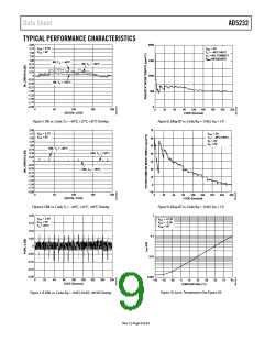
Typical Performance Characteristics ............................................. 9
Test Circuits..................................................................................... 12
Theory of Operation ...................................................................... 14
Scratch Pad and EEMEM Programming................................. 14
Basic Operation .......................................................................... 14
EEMEM Protection.................................................................... 14
Equipment Customer Start-up Sequence
for a PCB Calibrated Unit with Protected Settings................ 21
Flash/EEMEM Reliability.......................................................... 21
Evaluation Board ........................................................................ 21
Outline Dimensions....................................................................... 22
Ordering Guide .......................................................................... 22
REVISION HISTORY
Changes to Applications Section.....................................................1
Change to Wiper Resistance Parameter, Table 1...........................3
11/13—Rev. B to Rev. C
Changed t16 from 25 ms (max) to 25 ms (typ); Table 2 ............... 5
Changes to Ordering Guide .......................................................... 22
CS
Changes to
Rise to RDY Fall Time Parameter, Table 2...........5
Changes to Figure 2 and Figure 3....................................................6
Changes to Figure 24...................................................................... 12
Added Figure 32 ............................................................................. 13
Changes to Serial Data Interface Section .................................... 15
Changes to Programming the Variable Resistor Section .......... 19
Changes to Ordering Guide.......................................................... 22
09/11—Rev. A to Rev. B
Change to Resistor Noise Voltage Parameter in Table 1 ............. 4
10/09—Rev. 0 to Rev. A
Updated Format..................................................................Universal
Changes to Data Sheet Title ............................................................ 1
Changes to Features Section............................................................ 1
10/01—Revision 0: Initial Version
Rev. C | Page 2 of 24

 ADI [ ADI ]