AD1857/AD1858
O P ERATING FEATURES
Ser ial Input P or t Modes
Ser ial D ata Input P or t
T he AD1857/AD1858 use an input pin to control the mode
configuration of the input data port. MODE (Pin 3) programs
the input data port mode as follows:
T he AD1857/AD1858 use the frequency of the left/right and
master input clocks to determine the input sample rate. Gen-
erally, the master clock (MCLK) is divided down to synthesize
the left/right clock (LRCLK). LRCLK must run continuously
and transition twice per stereo sample period (except in the left-
justified DSP serial port style mode, when it transitions four
times per stereo sample period). T he bit clock (BCLK) is edge-
sensitive and may be used in a gated or burst mode, i.e., a
stream of pulses during data transmission followed by periods of
inactivity. T he bit clock is only used to write the audio data
into the serial input port. It is important that the left/right clock
is “clean,” with monotonic rising and falling edge transitions
and no excessive overshoot or undershoot that could cause false
clock triggering of the AD1857/AD1858.
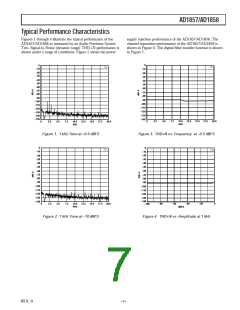
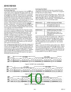
Figure 9 shows the AD1857 left-justified mode. LRCLK is HI
for the left channel, and LO for the right channel. Data is valid
on the rising edge of BCLK. T he MSB is left-justified to an
LRCLK transition, with no MSB delay. T he left-justified mode
can be used in the 16-, 18- or 20-bit input mode.
MODE (P in 3)
AD 1857 Serial Input P ort Mode
LO
HI
Left-Justified (See Figure 9)
I2S-Justified (See Figure 10)
T he AD1857/AD1858’s flexible serial data input port accepts
data in twos-complement, MSB first format. T he left channel
data field always precedes the right channel data field. T he
input data consists of 16, 18 or 20 bits (16 bits only to the
AD1858). All digital inputs are specified to T T L logic levels.
T he input data port is configured by a control pin, MODE,
Pin 3. T he AD1857 and the AD1858 are identical except for
the serial data input port modes offered. T he AD1857 offers
I2S-justified and left-justified modes, for 16-, 18- or 20-bit data
words. T he AD1858 offers right-justified and DSP serial port
style mode for 16-bit data words.
MODE (P in 3)
AD 1858 Serial Input P ort Mode
LO
HI
Right-Justified (See Figure 11)
Left-Justified DSP Serial Port Style
(See Figure 12)
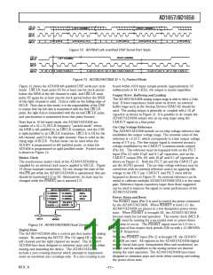
Figure 10 shows the AD1857 I2S-justified mode. LRCLK is
LO for the left channel, and HI for the right channel. Data is
valid on the rising edge of BCLK. T he MSB is left-justified to
an LRCLK transition, but with a single BCLK period delay.
T he I2S-justified mode can be used in the 16-, 18- or 20-bit
input mode.
Note: During the first 30,000 MCLK cycles after coming out of
reset, the AD1857/AD1858 synchronizes its internal sequencer
counter to the incoming LRCLK. After this period of time, it is
assumed that the LRCLK and the internal AD1857/AD1858
output channels could be switched (L to R and R to L). Therefore,
if the incoming LRCLK is stopped and then restarted with a
different phase, the AD1857/AD1858 should be reset again to
synchronize with this new clock.
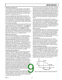
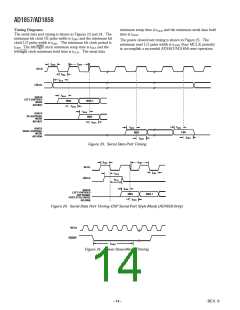
Figure 11 shows the AD1858 the right-justified mode. LRCLK
is HI for the left channel, and LO for the right channel. Data is
valid on the rising edge of BCLK. T he MSB is delayed 16-bit
clock periods from an LRCLK transition so that when there are
64 BCLK periods per LRCLK period, the LSB of the data will
be right-justified to the next LRCLK transition.
LRCLK
RIGHT CHANNEL
LEFT CHANNEL
INPUT
BCLK
INPUT
SDATA
MSB
MSB-1 MSB-2
MSB MSB-1 MSB-2
LSB+2 LSB+1
LSB
MSB
MSB-1
LSB+2 LSB+1
LSB
INPUT
Figure 9. AD1857 Left-J ustified Mode
LRCLK
INPUT
LEFT CHANNEL
RIGHT CHANNEL
BCLK
INPUT
SDATA
INPUT
MSB
MSB MSB-1 MSB-2
MSB MSB-1 MSB-2
LSB+2 LSB+1
LSB
LSB+2 LSB+1
LSB
Figure 10. AD1857 I2S-J ustified Mode
LRCLK
INPUT
RIGHT CHANNEL
LEFT CHANNEL
BCLK
INPUT
SDATA
INPUT
MSB MSB-1 MSB-2
MSB MSB-1 MSB-2
LSB
LSB+2 LSB+1 LSB
LSB+2 LSB+1 LSB
Figure 11. AD1858 Right-J ustified Mode
–10–
REV. 0

 ADI [ ADI ]