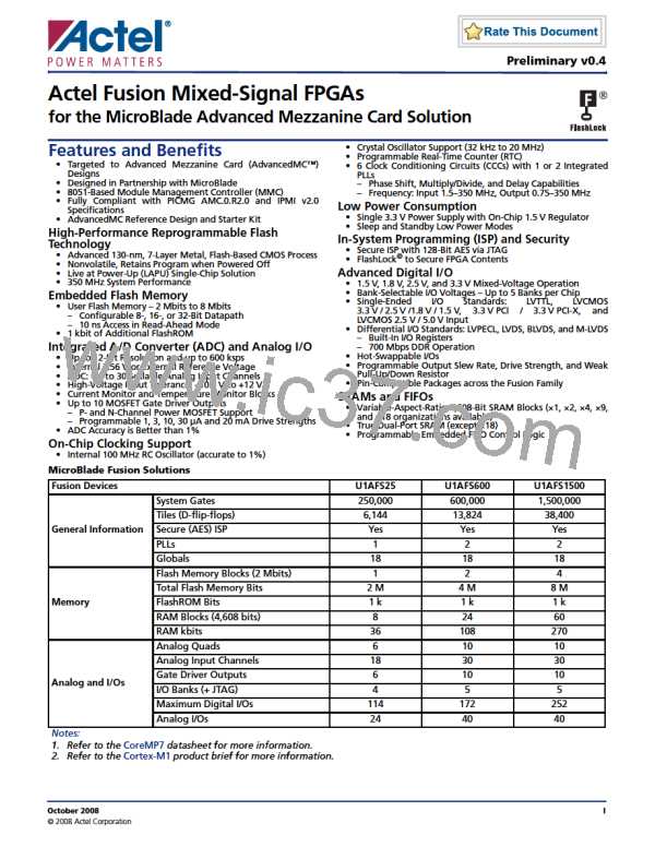
Actel Fusion Mixed-Signal FPGAs for the MicroBlade AdvancedMC Solution
was adopted by the National Institute of Standards and Technology (NIST) in 2000 and replaces the
DES standard, which was adopted in 1977. Fusion devices have a built-in AES decryption engine
and a flash-based AES key that make Fusion devices the most comprehensive programmable logic
device security solution available today. Fusion devices with AES-based security allow for secure
remote field updates over public networks, such as the Internet, and ensure that valuable IP
remains out of the hands of system overbuilders, system cloners, and IP thieves. As an additional
security measure, the FPGA configuration data of a programmed Fusion device cannot be read
back, although secure design verification is possible. During design, the user controls and defines
both internal and external access to the flash memory blocks.
Security, built into the FPGA fabric, is an inherent component of the Fusion family. The Flash cells
are located beneath seven metal layers, and many device design and layout techniques have been
used to make invasive attacks extremely difficult. Fusion with FlashLock and AES security is unique
in being highly resistant to both invasive and noninvasive attacks. Your valuable IP is protected,
making secure remote ISP possible. A Fusion device provides the most impenetrable security for
programmable logic designs.
Single Chip
Flash-based FPGAs store their configuration information in on-chip flash cells. Once programmed,
the configuration data is an inherent part of the FPGA structure, and no external configuration
data needs to be loaded at system power-up (unlike SRAM-based FPGAs). Therefore, flash-based
Fusion FPGAs do not require system configuration components such as EEPROMs or
microcontrollers to load device configuration data. This reduces bill-of-materials costs and PCB
area, and increases security and system reliability.
Live at Power-Up
Flash-based Fusion devices are Level 0 live at power-up (LAPU). LAPU Fusion devices greatly simplify
total system design and reduce total system cost by eliminating the need for CPLDs. The Fusion
LAPU clocking (PLLs) replaces off-chip clocking resources. The Fusion mix of LAPU clocking and
analog resources makes these devices an excellent choice for both system supervisor and system
management functions. LAPU from a single 3.3 V source enables Fusion devices to initiate, control,
and monitor multiple voltage supplies while also providing system clocks. In addition, glitches and
brownouts in system power will not corrupt the Fusion device flash configuration. Unlike SRAM-
based FPGAs, the device will not have to be reloaded when system power is restored. This enables
reduction or complete removal of expensive voltage monitor and brownout detection devices from
the PCB design. Flash-based Fusion devices simplify total system design and reduce cost and design
risk, while increasing system reliability.
Firm Errors
Firm errors occur most commonly when high-energy neutrons, generated in the upper atmosphere,
strike a configuration cell of an SRAM FPGA. The energy of the collision can change the state of the
configuration cell and thus change the logic, routing, or I/O behavior in an unpredictable way.
Another source of radiation-induced firm errors is alpha particles. For an alpha to cause a soft or
firm error, its source must be in very close proximity to the affected circuit. The alpha source must
be in the package molding compound or in the die itself. While low-alpha molding compounds are
being used increasingly, this helps reduce but does not entirely eliminate alpha-induced firm errors.
Firm errors are impossible to prevent in SRAM FPGAs. The consequence of this type of error can be
a complete system failure. Firm errors do not occur in Fusion Flash-based FPGAs. Once it is
programmed, the flash cell configuration element of Fusion FPGAs cannot be altered by high-
energy neutrons and is therefore immune to errors from them.
Recoverable (or soft) errors occur in the user data SRAMs of all FPGA devices. These can easily be
mitigated by using error detection and correction (EDAC) circuitry built into the FPGA fabric.
Low Power
Flash-based Fusion devices exhibit power characteristics similar to those of an ASIC, making them
an ideal choice for power-sensitive applications. With Fusion devices, there is no power-on current
surge and no high current transition, both of which occur on many FPGAs.
Fusion devices also have low dynamic power consumption and support both low power standby
mode and very low power sleep mode, offering further power savings.
Preliminary v0.4
1-3

 ACTEL [ Actel Corporation ]