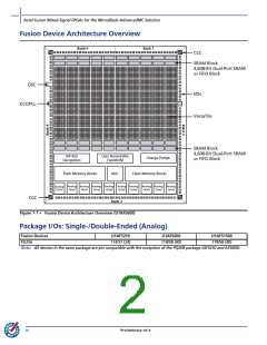
Fusion Device Family Overview
General Description
The Actel MicroBlade-based Fusion family, based on the highly successful ProASIC®3 and ProASIC3E
Flash FPGA architecture, has been designed as a high-performance, programmable, mixed-signal
platform. By combining an advanced flash FPGA core with flash memory blocks and analog
peripherals, Fusion devices dramatically simplify system design and, as a result, dramatically reduce
overall system cost and board space.
The state-of-the-art flash memory technology offers high-density integrated flash memory blocks,
enabling savings in cost, power, and board area relative to external flash solutions, while providing
increased flexibility and performance. The flash memory blocks and integrated analog peripherals
enable true mixed-mode programmable logic designs. Two examples are using an on-chip soft
processor to implement a fully functional Flash MCU and using high-speed FPGA logic to offer
system and power supervisory capabilities. Live at power-up and capable of operating from a single
3.3 V supply, the Fusion family is ideally suited for system management and control applications.
The devices in the Fusion family are categorized by FPGA core density. Each family member
contains many peripherals, including flash memory blocks, an analog-to-digital-converter (ADC),
high-drive outputs, both RC and crystal oscillators, and a real-time counter (RTC). This provides the
user with a high level of flexibility and integration to support a wide variety of mixed-signal
applications. The flash memory block capacity ranges from 2 Mbits to 8 Mbits. The integrated 12-
bit ADC supports up to 30 independently configurable input channels. The on-chip crystal and RC
oscillators work in conjunction with the integrated phase-locked loops (PLLs) to provide clocking
support to the FPGA array and on-chip resources. In addition to supporting typical RTC uses such as
watchdog timer, the Fusion RTC can control the on-chip voltage regulator to power down the
device (FPGA fabric, flash memory block, and ADC), enabling a low-power standby mode.
The Actel MicroBlade-based Fusion family offers revolutionary features, never before available in
an FPGA. The nonvolatile flash technology gives the Fusion solution the advantage of being a
secure, low-power, single-chip solution that is live at power-up. Fusion is reprogrammable and
offers time to market benefits at an ASIC-level unit cost. These features enable designers to create
high-density systems using existing ASIC or FPGA design flows and tools.
The family has up to 1.5 M system gates, supported with up to 270 kbits of true dual-port SRAM, up
to 8 Mbits of flash memory, 1 kbit of user FlashROM, and up to 278 user I/Os. With integrated flash
memory, the Fusion family is the ultimate soft-processor platform.
Flash Advantages
Reduced Cost of Ownership
Advantages to the designer extend beyond low unit cost, high performance, and ease of use. Flash-
based Fusion devices are live at power-up and do not need to be loaded from an external boot
PROM. On-board security mechanisms prevent access to the programming information and enable
secure remote updates of the FPGA logic. Designers can perform secure remote in-system
reprogramming to support future design iterations and field upgrades, with confidence that
valuable IP cannot be compromised or copied. Secure ISP can be performed using the industry-
standard AES algorithm with MAC data authentication on the device. The Fusion family device
architecture mitigates the need for ASIC migration at higher user volumes. This makes the Fusion
family a cost-effective ASIC replacement solution for applications in the consumer, networking and
communications, computing, and avionics markets.
Security
As the nonvolatile, flash-based Fusion family requires no boot PROM, there is no vulnerable
external bitstream. Fusion devices incorporate FlashLock, which provides a unique combination of
reprogrammability and design security without external overhead, advantages that only an FPGA
with nonvolatile flash programming can offer.
Fusion devices utilize a 128-bit flash-based key lock and a separate AES key to secure programmed
IP and configuration data. The FlashROM data in Fusion devices can also be encrypted prior to
loading. Additionally, the Flash memory blocks can be programmed during runtime using the
industry-leading AES-128 block cipher encryption standard (FIPS Publication 192). The AES standard
1-2
Preliminary v0.4

 ACTEL [ Actel Corporation ]