Actel Fusion Mixed-Signal FPGAs for the MicroBlade AdvancedMC Solution
Handbook. The flash memory parallel interface provides configurable byte-wide (×8), word-wide
(×16), or dual-word-wide (×32) data port options. Through the programmable flash parallel
interface, the on-chip and off-chip memories can be cascaded for wider or deeper configurations.
The flash memory has built-in security. The user can configure either the entire flash block or the
small blocks to prevent unintentional or intrusive attempts to change or destroy the storage
contents. Each on-chip flash memory block has a dedicated controller, enabling each block to
operate independently.
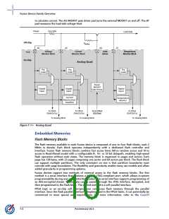
The flash block logic consists of the following sub-blocks:
•
•
•
•
Flash block – Contains all stored data. The flash block contains 64 sectors and each sector
contains 33 pages of data.
Page Buffer – Contains the contents of the current page being modified. A page contains 8
blocks of data.
Block Buffer – Contains the contents of the last block accessed. A block contains 128 data
bits.
ECC Logic – The flash memory stores error correction information with each block to
perform single-bit error correction and double-bit error detection on all data blocks.
User Nonvolatile FlashROM
In addition to the flash blocks, Actel Fusion devices have 1 kbit of user-accessible, nonvolatile
FlashROM on-chip. The FlashROM is organized as 8×128-bit pages. The FlashROM can be used in
diverse system applications:
•
•
•
•
•
•
•
•
Internet protocol addressing (wireless or fixed)
System calibration settings
Device serialization and/or inventory control
Subscription-based business models (for example, set-top boxes)
Secure key storage for secure communications algorithms
Asset management/tracking
Date stamping
Version management
The FlashROM is written using the standard IEEE 1532 JTAG programming interface. Pages can be
individually programmed (erased and written). On-chip AES decryption can be used selectively over
public networks to securely load data such as security keys stored in the FlashROM for a user
design.
The FlashROM can be programmed (erased and written) via the JTAG programming interface, and
its contents can be read back either through the JTAG programming interface or via direct FPGA
core addressing.
The FlashPoint tool in the Actel Fusion development software solutions, Libero IDE and Designer,
has extensive support for flash memory blocks and FlashROM. One such feature is auto-generation
of sequential programming files for applications requiring a unique serial number in each part.
Another feature allows the inclusion of static data for system version control. Data for the
FlashROM can be generated quickly and easily using the Actel Libero IDE and Designer software
tools. Comprehensive programming file support is also included to allow for easy programming of
large numbers of parts with differing FlashROM contents.
SRAM and FIFO
Fusion devices have embedded SRAM blocks along the north and south sides of the device. Each
variable-aspect-ratio SRAM block is 4,608 bits in size. Available memory configurations are 256×18,
512×9, 1k×4, 2k×2, and 4k×1 bits. The individual blocks have independent read and write ports that
can be configured with different bit widths on each port. For example, data can be written
through a 4-bit port and read as a single bitstream. The SRAM blocks can be initialized from the
flash memory blocks or via the device JTAG port (ROM emulation mode), using the UJTAG macro.
In addition, every SRAM block has an embedded FIFO control unit. The control unit allows the
SRAM block to be configured as a synchronous FIFO without using additional core VersaTiles. The
FIFO width and depth are programmable. The FIFO also features programmable Almost Empty
Preliminary v0.4
1-7

 ACTEL [ Actel Corporation ]