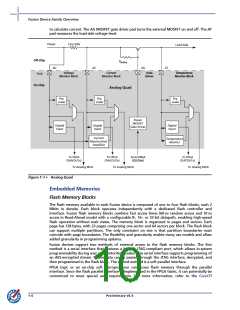
Fusion Device Family Overview
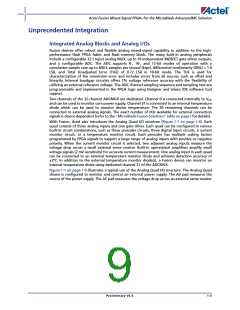
to calculate current. The AG MOSFET gate driver pad turns the external MOSFET on and off. The AT
pad measures the load-side voltage level.
Power
Line Side
Load Side
Off-Chip
Rpullup
AV
AC
AG
AT
Voltage
Monitor Block
Current
Monitor Block
Gate
Driver
Temperature
Monitor Block
Pads
On-Chip
Analog Quad
Pre-
scaler
Pre-
scaler
Pre-
scaler
Power
MOSFET
Gate Driver
Digital
Input
Digital
Input
Digital
Input
Current
Monitor/Instr
Amplifier
Temperature
Monitor
To FPGA
(DAVOUTx)
To FPGA
(DACOUTx)
From FPGA
(GDONx)
To FPGA
(DATOUTx)
To Analog MUX
To Analog MUX
To Analog MUX
Figure 1-1 • Analog Quad
Embedded Memories
Flash Memory Blocks
The flash memory available in each Fusion device is composed of one to four flash blocks, each 2
Mbits in density. Each block operates independently with a dedicated flash controller and
interface. Fusion flash memory blocks combine fast access times (60 ns random access and 10 ns
access in Read-Ahead mode) with a configurable 8-, 16-, or 32-bit datapath, enabling high-speed
flash operation without wait states. The memory block is organized in pages and sectors. Each
page has 128 bytes, with 33 pages comprising one sector and 64 sectors per block. The flash block
can support multiple partitions. The only constraint on size is that partition boundaries must
coincide with page boundaries. The flexibility and granularity enable many use models and allow
added granularity in programming updates.
Fusion devices support two methods of external access to the flash memory blocks. The first
method is a serial interface that features a built-in JTAG-compliant port, which allows in-system
programmability during user or monitor/test modes. This serial interface supports programming of
an AES-encrypted stream. Secure data can be passed through the JTAG interface, decrypted, and
then programmed in the flash block. The second method is a soft parallel interface.
FPGA logic or an on-chip soft microprocessor can access flash memory through the parallel
interface. Since the flash parallel interface is implemented in the FPGA fabric, it can potentially be
customized to meet special user requirements. For more information, refer to the CoreCFI
1-6
Preliminary v0.4

 ACTEL [ Actel Corporation ]