Device Architecture
Features Supported on Pro I/Os
Table 2-69 lists all features supported by transmitter/receiver for single-ended and differential
I/Os.
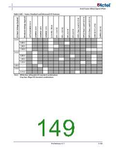
Table 2-69 • Fusion Pro I/O Features
Feature
Single-ended and voltage- • Hot insertion in every mode except PCI or 5 V input tolerant (these modes
Description
referenced transmitter
features
use clamp diodes and do not allow hot insertion)
Activation of hot insertion (disabling the clamp diode) is selectable by I/Os.
Weak pull-up and pull-down
•
•
•
•
Two slew rates
Skew between output buffer enable/disable time: 2 ns delay (rising edge)
and 0 ns delay (falling edge); see "Selectable Skew between Output Buffer
Enable/Disable Time" on page 2-148 for more information
•
•
•
Five drive strengths
5 V–tolerant receiver ("5 V Input Tolerance" section on page 2-143)
LVTTL/LVCMOS 3.3 V outputs compatible with 5 V TTL inputs ("5 V Output
Tolerance" section on page 2-146)
•
High performance (Table 2-73 on page 2-141)
Single-ended receiver features • Schmitt trigger option
•
•
ESD protection
Programmable delay: 0 ns if bypassed, 0.625 ns with '000' setting, 6.575 ns
with '111' setting, 0.85-ns intermediate delay increments (at 25°C, 1.5 V)
•
•
High performance (Table 2-73 on page 2-141)
Separate ground planes, GND/GNDQ, for input buffers only to avoid
output-induced noise in the input circuitry
Voltage-referenced
differential receiver features
•
Programmable Delay: 0 ns if bypassed, 0.625 ns with '000' setting, 6.575 ns
with '111' setting, 0.85-ns intermediate delay increments (at 25°C, 1.5 V)
•
•
High performance (Table 2-73 on page 2-141)
Separate ground planes, GND/GNDQ, for input buffers only to avoid
output-induced noise in the input circuitry
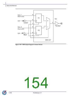
CMOS-style
M-LVDS, or LVPECL
transmitter
LVDS,
BLVDS, • Two I/Os and external resistors are used to provide a CMOS-style LVDS,
BLVDS, M-LVDS, or LVPECL transmitter solution.
•
•
•
•
•
•
Activation of hot insertion (disabling the clamp diode) is selectable by I/Os.
Weak pull-up and pull-down
Fast slew rate
LVDS/LVPECL differential
receiver features
ESD protection
High performance (Table 2-73 on page 2-141)
Programmable delay: 0.625 ns with '000' setting, 6.575 ns with '111'
setting, 0.85-ns intermediate delay increments (at 25°C, 1.5 V)
•
Separate input buffer ground and power planes to avoid output-induced
noise in the input circuitry
2-134
Preliminary v1.7

 ACTEL [ Actel Corporation ]