Actel Fusion Mixed-Signal FPGAs
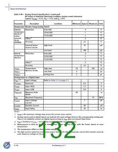
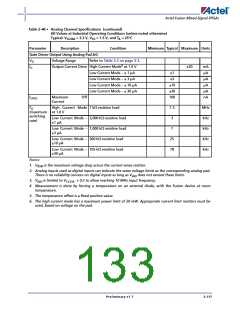
Table 2-46 • Analog Channel Specifications (continued)
All Values at Industrial Operating Conditions (unless noted otherwise)
Typical: VCC33A = 3.3 V, VCC = 1.5 V, and TA = 25°C
Parameter
Description
Condition
Minimum Typical Maximum Units
Gate Driver Output Using Analog Pad AG
VG
IG
Voltage Range
Output Current Drive High Current Mode6 at 1.0 V
Refer to Table 3-2 on page 3-3.
20
mA
µA
µA
µA
µA
nA
Low Current Mode – 1 µA
1
3
Low Current Mode – 3 µA
Low Current Mode – 10 µA
10
30
100
Low Current Mode – 30 µA
IOFFG
FG
Maximum
Current
Off
High Current Mode 1 kΩ resistive load
1.3
3
MHz
kHz
kHz
kHz
kHz
(maximum at 1.0 V
switching
rate)
Low Current Mode – 3,000 kΩ resistive load
1 µA
Low Current Mode – 1,000 kΩ resistive load
3 µA
7
Low Current Mode – 300 kΩ resistive load
10 µA
25
78
Low Current Mode – 105 kΩ resistive load
30 µA
Notes:
1. VRSM is the maximum voltage drop across the current sense resistor.
2. Analog inputs used as digital inputs can tolerate the same voltage limits as the corresponding analog pad.
There is no reliability concern on digital inputs as long as VIND does not exceed these limits.
3. VIND is limited to VCC33A + 0.2 to allow reaching 10 MHz input frequency.
4. Measurement is done by forcing a temperature on an external diode, with the Fusion device at room
temperature.
5. The temperature offset is a fixed positive value.
6. The high current mode has a maximum power limit of 20 mW. Appropriate current limit resistors must be
used, based on voltage on the pad.
Preliminary v1.7
2-117

 ACTEL [ Actel Corporation ]