Actel Fusion Mixed-Signal FPGAs
Analog System Characteristics
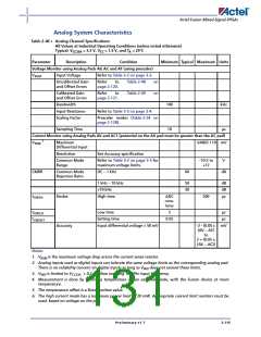
Table 2-46 • Analog Channel Specifications
All Values at Industrial Operating Conditions (unless noted otherwise)
Typical: VCC33A = 3.3 V, VCC = 1.5 V, and TA = 25°C
Parameter
Description
Condition
Minimum Typical Maximum Units
Voltage Monitor using Analog Pads AV, AC and AT (using prescaler)
VINAP
Input Voltage
Refer to Table 3-2 on page 3-3.
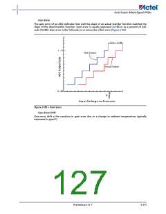
Uncalibrated Gain
and Offset Errors
Refer
page 2-120.
to
Table 2-48
on
on
Calibrated Gain
and Offset Errors
Refer to
page 2-121.
Table 2-49
Bandwidth
100
10
kHz
µs
Input Resistance
Scaling Factor
Refer to Table 3-3 on page 3-4.
Prescaler modes (Table 2-54 on
page 2-128).
Sampling Time
Current Monitor using Analog Pads AV and AC1 (potential on the AV pad must be greater than the AC pad)
1
VRSM
Maximum
VAREF / 10 mV
Differential Input
Resolution
See Accuracy specification
Common Mode
Range
Refer to Table 3-2 on page 3-3 for
maximum voltage limits.
–10.5 to
+12
V
CMRR
Common Mode
Rejection Ratio
DC – 1 kHz
60
dB
1 kHz – 10 kHz
>10 kHz
50
30
dB
dB
µs
tCMSHI
Strobe
High time
ADC
conv.
time
200
tCMSLO
tCMSSET
Low time
5
µs
µs
Setting time
0.02
Accuracy
Input differential voltage > 50 mV
–2 – (0.05 × mV
(AV – AC)
to
2 + (0.05 ×
(AV – AC))
Notes:
1. VRSM is the maximum voltage drop across the current sense resistor.
2. Analog inputs used as digital inputs can tolerate the same voltage limits as the corresponding analog pad.
There is no reliability concern on digital inputs as long as VIND does not exceed these limits.
3. VIND is limited to VCC33A + 0.2 to allow reaching 10 MHz input frequency.
4. Measurement is done by forcing a temperature on an external diode, with the Fusion device at room
temperature.
5. The temperature offset is a fixed positive value.
6. The high current mode has a maximum power limit of 20 mW. Appropriate current limit resistors must be
used, based on voltage on the pad.
Preliminary v1.7
2-115

 ACTEL [ Actel Corporation ]