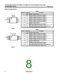
BATTERY PROTECTION IC FOR 2-SERIAL TO 4-SERIAL-CELL PACK (SECONDARY PROTECTION)
S-8264A/B/C Series
Rev.4.4_00
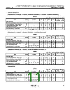
Test Circuits
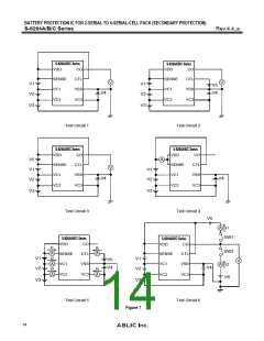
(1) Test Condition 1, Test Circuit 1
Set V1, V2, V3, and V4 to 3.5 V. Overcharge detection voltage 1 (VCU1) is the V1 voltage when CO is “H” after the
voltage of V1 has been gradually increased. The overcharge hysteresis voltage (VHC1) is the difference between V1
and VCU1 when CO is “L” after the voltage of V1 has been gradually decreased.
Overcharge detection voltage VCUn (n = 2 to 4) and overcharge hysteresis VHCn (n = 2 to 4) can be determined in the
same way as when n = 1.
(2) Test Condition 2, Test Circuit 1
Set V1, V2, V3, and V4 to 3.5 V and in a moment of time (within 10 μs) increase V1 up to 5.0 V. The overcharge
detection delay time (tCU) is the period from when V1 reached 5.0 V to when CO becomes “H”. After that, in a moment
of time (within 10 μs) decrease V1 down to 3.5 V. The overcharge release delay time (tCL) is the period from when V1
has reached 3.5 V to when CO becomes “L”.
(3) Test Condition 3, Test Circuit 1
Set V1, V2, V3, and V4 to 3.5 V and in a moment of time (within 10 μs) increase V1 up to 5.0 V. This is defined as the
first rise. Within tCU − 20 ms after the first rise, in a moment of time (within 10 μs) decrease V1 down to 3.5 V and then
in a moment of time (within 10 μs) restore up to 5.0 V. This is defined as the second rise. When the period from when
V1 was fallen to the second rise is short, CO becomes “H” after tCU has elapsed since the first rise. If the period from
when V1 falls to the second rise is gradually made longer, CO becomes “H” when tCU has elapsed since the second rise.
The overcharge timer reset delay time (tTR) is the period from V1 fall till the second rise at that time.
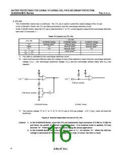
(4) Test Condition 4, Test Circuit 2
In the S-8264A/C Series, set V1, V2, V3, and V4 to 3.5 V and V5 to 14 V. The CTL pin response time (tCTL) is the period
from when V5 reaches 0 V after V5 is in a moment of time (within 10 μs) decreased down to 0 V to when CO becomes
“H”.
In the S-8264B Series, set V1, V2, V3, and V4 to 3.5 V and V5 to 14 V after an overvoltage is detected and CO becomes
“H”. In a moment of time (within 10 μs) raise V5 from 0 V to 14 V. The CTL pin response time (tCTL) is the period from
when V5 becomes 14 V to when CO becomes “L”.
(5) Test Condition 5, Test Circuit 3
After setting V1, V2, V3, and V4 to 3.5 V and V5 to 0 V, in a moment of time (within 10 μs) increase V5 up to 8.5 V and
decrease V5 again down to 0 V. When the period from when V5 was raised to when it has fallen is short, if an
overcharge detection operation is performed subsequently, the overcharge detection time is tCU. However, when the
period from when V5 is raised to when it is fallen is gradually made longer, the overcharge detection time during the
subsequent overcharge detection operation is shorter than tCU. The transition time to test mode (tTST) is the period from
when V5 was raised to when it has fallen at that time.
12

 ABLIC [ ABLIC ]