0.27
A CURRENT CONSUMPTION VOLTAGE DETECTOR WITH DELAY FUNCTION (EXTERNAL DELAY TIME SETTING)
S-1009 Series
Rev.5.1_03
Operation
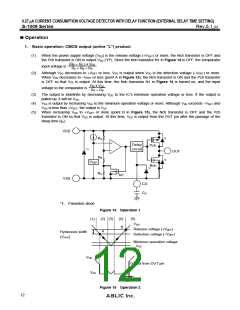
1. Basic operation: CMOS output (active "L") product
(1)
(2)
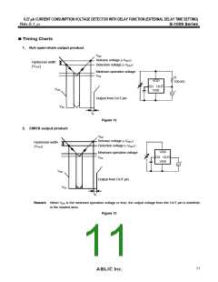
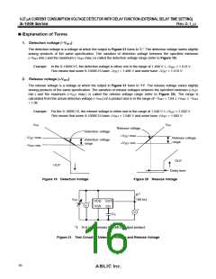
When the power supply voltage (VDD) is the release voltage (VDET) or more, the Nch transistor is OFF and
the Pch transistor is ON to output VDD ("H"). Since the Nch transistor N1 in Figure 14 is OFF, the comparator
(RB RC ) VDD
RA RB RC
input voltage is
.
Although VDD decreases to VDET or less, VDD is output when VDD is the detection voltage (VDET) or more.
When VDD decreases to VDET or less (point A in Figure 15), the Nch transistor is ON and the Pch transistor
is OFF so that VSS is output. At this time, the Nch transistor N1 in Figure 14 is turned on, and the input
RB VDD
voltage to the comparator is
.
RA RB
The output is indefinite by decreasing VDD to the IC’s minimum operation voltage or less. If the output is
pulled up, it will be VDD
VSS is output by increasing VDD to the minimum operation voltage or more. Although VDD exceeds VDET and
VDD is less than VDET, the output is VSS
(3)
(4)
(5)
.
.
When increasing VDD to VDET or more (point B in Figure 15), the Nch transistor is OFF and the Pch
transistor is ON so that VDD is output. At this time, VDD is output from the OUT pin after the passage of the
delay time (tD).
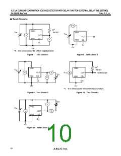
VDD
*1
RA
Delay
circuit
Pch
Nch
*1
OUT
RB
RC
*1
VREF
*1
N1
VSS
CD
CD
*1. Parasiteic diode
Figure 14 Operation 1
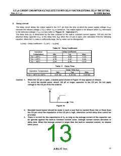
(2) (3)
A
(4)
B
(5)
VDD
(1)
Release voltage (VDET
)
Hysteresis width
Detection voltage (VDET
)
(VHYS
)
Minimum operation voltage
VSS
VDD
Output from OUT pin
VSS
tD
Figure 15 Operation 2
12

 ABLIC [ ABLIC ]