0.27
A CURRENT CONSUMPTION VOLTAGE DETECTOR WITH DELAY FUNCTION (EXTERNAL DELAY TIME SETTING)
S-1009 Series
Rev.5.1_03
Explanation of Terms
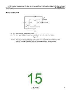
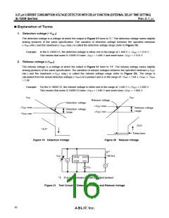
1. Detection voltage (VDET
)
The detection voltage is a voltage at which the output in Figure 21 turns to "L". The detection voltage varies slightly
among products of the same specification. The variation of detection voltage between the specified minimum
(VDET min.) and the maximum (VDET max.) is called the detection voltage range (refer to Figure 19).
Example: In the S-1009C15, the detection voltage is either one in the range of 1.488 V VDET 1.512 V.
This means that some S-1009C15 have VDET = 1.488 V and some have VDET = 1.512 V.
2. Release voltage (VDET
)
The release voltage is a voltage at which the output in Figure 21 turns to "H". The release voltage varies slightly
among products of the same specification. The variation of release voltages between the specified minimum (VDET
min.) and the maximum (VDET max.) is called the release voltage range (refer to Figure 20). The range is
calculated from the actual detection voltage (VDET) of a product and is in the range of VDET 1.04 VDET VDET
1.06.
Example: For the S-1009C15, the release voltage is either one in the range of 1.548 V VDET 1.602 V.
This means that some S-1009C15 have VDET = 1.548 V and some have VDET = 1.602 V.
VDD
VDD
Release voltage
Detection voltage
VDET max.
VDET min.
VDET max.
VDET min.
Release voltage
range
Detection voltage
range
OUT
OUT
Delay time
Figure 20 Release Voltage
Figure 19 Detection Voltage
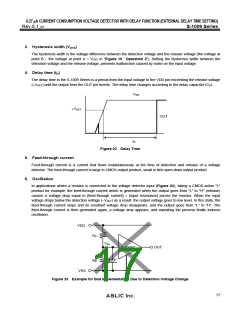
R*1
VDD
100 k
VDD OUT
V
VSS
CD
V
CD
*1. R is unnecessary for CMOS output product.
Figure 21 Test Circuit of Detection Voltage and Release Voltage
16

 ABLIC [ ABLIC ]