0.27
A CURRENT CONSUMPTION VOLTAGE DETECTOR WITH DELAY FUNCTION (EXTERNAL DELAY TIME SETTING)
S-1009 Series
Rev.5.1_03
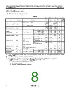
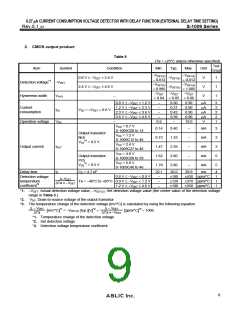
Electrical Characteristics
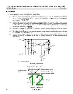
1. Nch open-drain output product
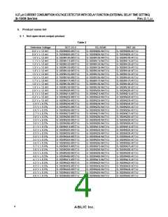
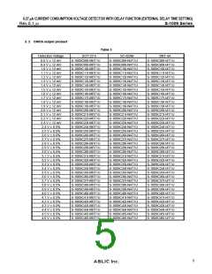
Table 8
(Ta = 25°C unless otherwise specified)
Test
Circuit
Item
Symbol
Condition
0.8 V VDET 2.4 V
2.4 V VDET 4.6 V
Min.
Typ.
Max.
Unit
V
VDET(S)
0.012
VDET(S)
0.995
VDET
VDET(S)
0.012
VDET(S)
1.005
VDET
VDET(S)
1
Detection voltage*1 VDET
VDET(S)
VDET
V
1
1
Hysteresis width
VHYS
V
0.04 0.05 0.06
0.8 V VDET 1.2 V
1.2 V VDET 2.3 V
2.3 V VDET 3.6 V
3.6 V VDET 4.6 V
VDD = 0.7 V
S-1009N08 to 14
VDD = 1.2 V
0.7
0.30
0.27
0.42
0.39
0.90
0.90
0.90
0.90
10.0
A
A
A
A
V
2
2
2
2
1
Current
consumption
ISS
VDD = VDET 0.6 V
Operation voltage
Output current
VDD
0.14
0.73
1.47
0.40
1.33
2.39
mA
mA
mA
3
3
3
Output transistor
Nch
IOUT
S-1009N15 to 46
VDD = 2.4 V
S-1009N27 to 46
VDS*2 = 0.5 V
Output transistor
Nch
Leakage current
Delay time
ILEAK
tD
0.08
29.9
A
3
V
DD = 10.0 V, VOUT = 10.0 V
CD = 4.7 nF
22.1
26.0
180
120
100
ms
4
1
1
1
0.8 V VDET 0.9 V
430 ppm/°C
370 ppm/°C
350 ppm/°C
Detection voltage
temperature
VDET
Ta VDET
Ta = 40°C to 85°C 0.9 V VDET 1.2 V
1.2 V VDET 4.6 V
coefficient*3
*1. VDET: Actual detection voltage value, VDET(S): Set detection voltage value (the center value of the detection voltage
range in Table 2.)
*2.
VDS: Drain-to-source voltage of the output transistor
*3. The temperature change of the detection voltage [mV/°C] is calculated by using the following equation.
VDET
Ta
VDET
Ta VDET
mV/°C *1 = VDET(S) (typ.) V *2
ppm/°C *3 1000
]
[
]
[ ]
[
*1. Temperature change of the detection voltage
*2. Set detection voltage
*3. Detection voltage temperature coefficient
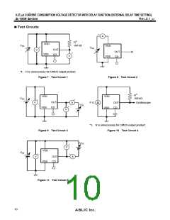
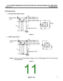
8

 ABLIC [ ABLIC ]