AP4525GEH-A
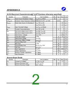
N-CH Electrical Characteristics@ Tj=25oC(unless otherwise specified)
Symbol
BVDSS
Parameter
Test Conditions
VGS=0V, ID=250uA
Min. Typ. Max. Units
Drain-Source Breakdown Voltage
40
-
-
-
-
V
V/℃
mΩ
mΩ
V
ΔBVDSS/ΔTj
Breakdown Voltage Temperature Coefficient Reference to 25℃, ID=1mA
0.03
RDS(ON)
Static Drain-Source On-Resistance2 VGS=10V, ID=6A
-
-
-
26
32
3
V
GS=4.5V, ID=4A
-
VGS(th)
Gate Threshold Voltage
VDS=VGS, ID=250uA
VDS=10V, ID=6A
1
-
-
gfs
Forward Transconductance
Drain-Source Leakage Current (Tj=25oC)
Drain-Source Leakage Current (Tj=70oC)
Gate-Source Leakage
Total Gate Charge2
6
-
S
IDSS
uA
uA
uA
nC
nC
nC
ns
ns
ns
ns
pF
pF
pF
Ω
VDS=40V, VGS=0V
VDS=32V, VGS=0V
VGS=±16V
ID=6A
-
-
-
-
-
-
-
-
-
-
-
-
-
-
-
-
1
25
IGSS
Qg
-
±30
9
14
-
Qgs
Qgd
td(on)
tr
Gate-Source Charge
Gate-Drain ("Miller") Charge
Turn-on Delay Time2
Rise Time
VDS=20V
1.5
4
VGS=4.5V
VDS=20V
-
7
-
ID=6A
20
20
4
-
td(off)
tf
Turn-off Delay Time
RG=3Ω,VGS=10V
RD=3.3Ω
-
Fall Time
-
Ciss
Coss
Crss
Rg
Input Capacitance
VGS=0V
580 930
Output Capacitance
Reverse Transfer Capacitance
Gate Resistance
VDS=25V
100
70
2
-
-
f=1.0MHz
f=1.0MHz
3
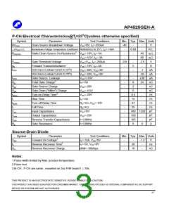
Source-Drain Diode
Symbol
Parameter
Test Conditions
Min. Typ. Max. Units
VSD
trr
Forward On Voltage2
Reverse Recovery Time2
IS=15A, VGS=0V
IS=6A, VGS=0V
dI/dt=100A/µs
-
-
-
-
1.3
V
20
15
-
-
ns
nC
Qrr
Reverse Recovery Charge
2/7

 A-POWER [ ADVANCED POWER ELECTRONICS CORP. ]