W89C840F
Pin Function Descriptions
1) PCI Interface
Signal Name
Pin
Pin
Pin Description
Type
Number
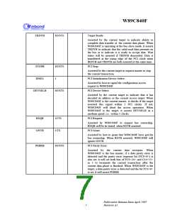
PCICLK
I
I
PCI Clock Input:
The W89C840F supports PCI clock rate ranged from
25Mhz to 33MHz continuously. All PCI signals except
RST# and INTA#, are referenced on the rising edge of
this clock.
RSTB
Hardware reset signal:
When asserted(active low), all PCI output of W89C840F
will be in high impedance state, and all open drain
signals will be floated. The configurations inside
W89C840F will be in its initial state. This signal must
be asserted for a period of, at least, 10 PCI clocks to
have a reset on hardware correctly.
AD[31:0]
C_BEB[3:0]
PAR
IO/TS
IO/TS
IO/TS
IO/STS
Multiplexed Address and Data bus:
During the first cycle that FRAME# asserts, they act as
an address bus; on the other cycles, they are switched to
be a data bus.
Multiplexed command and byte enables:
These signals are driven by current bus master. During
address phase, it means a bus command; on the other
phase, it presents byte enable of the transaction.
Parity signal.
This PAR represents even parity across AD[31:0] and
C_BEB[3:0]. It has the same timing as AD[31:0] but
delayed by one clock.
FRAMEB
PCI Cycle Frame:
The current bus master asserts FRAMEB to indicate the
beginning and duration of a bus access. This signal will
keep asserted while the current transaction is ongoing
and will keep deasserted to indicate that the next data
phase is the final data phase.
IRDYB
IO/STS
Initiator Ready:
The IRDYB asserted by the current initiator to indicate
the ability to complete the data transfer at the current
data phase. The initiator asserts IRDYB to indicate the
valid write data, or to indicate it is ready to accept the
read data. More than or exactly one wait state will be
inserted if IRDYB deasserted during the current
transaction. Data is transferred at the clock rising edge
when both IRDYB and TRDYB are asserted at the same
time.
- 6 -

 ETC [ ETC ]