BRIGHT
Microelectronics
Inc.
BM29F400T/BM29F400B
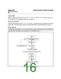
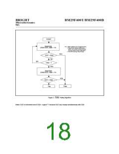
The DQ5 failure condition may also appear if a user tries to program a non blank location without
erasing. In this case, the device may exceed time limits and not complete the Internal Algorithm
operation. Hence, the system never reads a valid data on DQ7 bit and DQ6 never stops toggling.
Once the device has exceeded timing limits, the DQ5 bit will indicate a "1".
DQ3
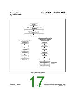
Sector Erase Timer
After the completion of the initial Sector Erase command sequence, the sector erase time-out window
will begin. DQ3 will remain low until the time-out window is closed. Data Polling and Toggle Bit are
valid after the initial Sector Erase command sequence.
Data
If
Polling or the Toggle Bit indicates the device has been written with a valid erase command,
DQ3 maybe used to determine if the Sector Erase time-out window is still open. If DQ3 is a logical
"1", the internally controlled erase cycle has begun. Attempts to write subsequent command to the
device will be ignored until the erase operation is completed as indicated by Data Polling or Toggle
Bit. If DQ3 is a logical "0", the device will accept additional Sector Erase commands. To ensure the
command has been accepted, the system software should check the status of DQ3 prior to and
following each subsequent Sector Erase command. If DQ3 were high on the second status check, the
command may not have been accepted. Refer to Table 7: Write Operation Status Flags.
Write Operations Status
STATUS
DQ7
DQ6
DQ5
DQ3
In
Byte/Word Programming Operation
Toggle
0
N/A
DQ7
0
Progress
Chip or Sector Erase Operation
Toggle
Data
0
1
Erase Suspend Mode
Data
Data
Data
(Non-Erase Suspended Sector)
Exceeded
Byte/Word Programming Operation
Toggle
Toggle
1
1
0
1
DQ7
0
Time Limits
Chip or Sector Erase Operation
Table 7. Write Operation Status Flags(1)
Notes: DQ0, DQ1, DQ4 are reserve pins for future use.
RY/BY
Ready/Busy Status
The BM29F400 provides a RY/BY open-drain output pin as a way to indicate to the host system that
an Internal Programming or Erase operation is either in progress or has been completed. If the RY/BY
output is low, the device is busy with either a Programming or Erase operation. If the RY/BY output is
high, the device is ready to accept a Read, Programming, or Erase command. When the RY/BY pin
is low, the device will not accept any additional Programming or Erase commands with the exception
of the Erase Suspend command. If the BM29F400 is placed in an Erase Suspend mode, the RY/BY
output will be high.
- 14 -

 WINBOND [ WINBOND ]