BRIGHT
Microelectronics
Inc.
BM29F400T/BM29F400B
Data
The
Polling feature is only active during the Byte/Word Programming operation, Chip Erase
operation, Sector Erase Operation, or Sector Erase time-out window (see Table 7).
DQ6
Toggle Bit
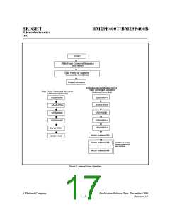
The BM29F400 also features the "Toggle Bit" as a method to indicate to the host system the status of
the Internal Programming and Erase Algorithms (see Figure 4 for Toggle Bit (DQ6) flowchart.
OE
During an Internal Programming or Erase Algorithm cycle, successive attempts to read (
toggling)
data from the device will result in DQ6 toggling between one and zero. Once Internal Programming or
Erase operation is completed, DQ6 will stop toggling and valid data will be read on the next
BYTE
successive attempts. During
Programming, Toggle Bit is valid after the rising edge of the
pulse in the four write pulse sequence. For Chip Erase, Toggle Bit is valid after the rising
WE
WE
fourth
edge of the sixth
pulse in the six write pulse sequence. For Sector Erase, Toggle Bit is valid after
WE
the last rising edge of the sector erase
out window.
pulse. Toggle Bit is also active during sector erase time-
In Byte/Word Programming, if the sector being written to is protected, the Toggle Bit will toggle for
about 300 nS and then stop toggling without the data having changed. In Chip Erase or Sector Erase,
the device will erase all the selected sectors except for the ones that are protected. If all selected
sectors are protected, the chip will toggle the Toggle Bit for about 300 nS and then drop back into
CE
OE
toggling will cause the DQ6 Toggle
read mode, having changed none of the data. Either
Bit I to toggle.
or
DQ5
Exceeded Timing Limits
DQ5 will indicate if the Byte/Word Programming, Chip Erase, or Sector Erase time has exceeded the
specified limits (internal pulse count) of the device. Under these conditions DQ5 will produce a logical
"1". This is a failure condition which indicates that the program or erase cycle was not successfully
OE
Data
completed.
Polling is the only operating function of the device under this condition. The
WE
and
pins will control the output disable functions as described in Table 1.
If this failure condition occurs during Sector Erase operation, it specifies that particular sector is bad
and it may not be reused. However, other sectors are still functional and may continue to be used for
RESET
the program or erase operation. The device must be
to the Read mode to use other sectors
of the device. Write the Read/Reset command sequence to the device, and then execute the
Byte/Word Programming or Sector Erase command sequence. This allows the system to continue to
use the other active sectors in the device.
If this failure condition occurs during Chip Erase operation, it specifies that the entire chip is bad or
combination of sectors are bad. In so, the chip should not be reused.
If this failure condition occurs during Byte/Word Programming operation, it indicates the entire sector
BYTE
containing that
can be reused.)
is bad and this sector may not be reused (other sectors are still functional and
A Winbond Company
Publication Release Date: December 1999
- 13 -
Revision A2

 WINBOND [ WINBOND ]