BRIGHT
Microelectronics
Inc.
BM29F400T/BM29F400B
WE
WE
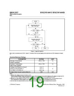
During a programming operation, the RY/BY pin is driven low after the rising edge of the fourth
pulse. During an erase operation, the RY/BY pin is driven low after the rising edge of the sixth
RESET
pulse. The RY/BY pin will indicate a busy condition during the
pulse. Refer to the timing
waveforms for the RY/BY status pin for further clarification. The RY/BY pin is high in the Standby
mode.
Since this is an open-drain output, several RY/BY pins can be tied together with a pull-up resistor to
Vcc.
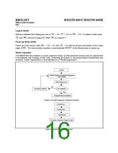
RESET Hardware Reset
IL
RESET
RESET
RESET
pin must be
The BM29F400 device may be
by driving the
pin to V . The
IL
RESET
kept low (V ) for at least 500 nS. Pulling the
pin low will terminate any operation in progress.
RESET
RESET
pin is
The internal state machine will be
RESET
to the read mode 1 mS to 230 mS after the
driven low. If a hardware
occurs during a Programming or Erase operation, the data at that
particular location will be indeterminate.
RESET
RESET
is complete, the device goes to Standby mode
When the
and cannot be accessed. Also, note that all the data output pins are tri-stated for the duration of the
RESET RESET
pin is low and the internal
pulse. Once the
pin is taken high, the device requires 500 nS of wake up time until
outputs are valid for a read access.
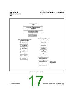
RESET
RESET
RESET
RESET
The
pin may be tied to the system
input. Therefore, if a system
occurs
to read
during an Internal Programming or Erase operation, the device will be automatically
mode. This will enable the system's microprocessor to read the boot-up firmware from the Flag's
memory.
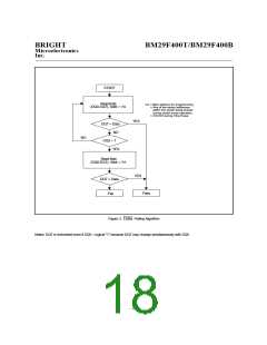
Data Protection
The BM29F400 is designed to offer protection against accidental erasure or programming caused by
spurious system level signals that may exist during power transitions. During power-up the device
automatically resets the internal state machine in the Read mode. Also, with its control register
architecture, alteration of the memory contents only occurs after successful completion of specific
multi-bus cycle command sequences. The device also incorporates several features to prevent
inadvertent write cycles resulting from Vcc power-up and power-down transitions or system noise.
Low Vcc Write Inhibit
To avoid initiation of a write cycle during Vcc power-up and power-down, a write cycle is locked out
LKO
for Vcc less than 3.2V (typically 3.7V). If Vcc < V
, the command register is disabled and all
RESET
to the
. It is the users
internal programming/erase circuits are disabled. Under this condition the device will
LKO
Read mode. Subsequent writes will be ignored until the Vcc level is greater than V
responsibility to ensure that the control pins are logically correct to prevent unintentional writes when
Vcc is above 3.2V.
Write Pulse "Glitch" Protection
OE CE
WE
will not initiate a write cycle.
Noise pulses of less than 5 nS (typical) on
,
or
A Winbond Company
Publication Release Date: December 1999
Revision A2
- 15 -

 WINBOND [ WINBOND ]