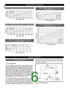
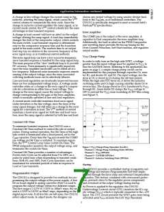
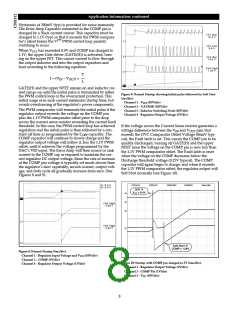
Typical Performance Characteristics
Figure 1: Gate(H) and Gate(L) Falltime vs. Load Capacitance.
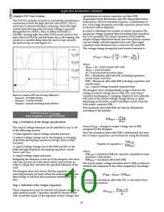
Figure 4: Percent Output Error vs. DAC Output
Voltage Setting, VID4 = 0.
150
V
= 12V
= 25°C
0.10
0.05
0
125
100
75
50
25
0
CC
T
A
−0.05
−0.10
−0.15
−0.20
V
= 12V
CC
T
A
= 25°C
V
ID4
= 0
0
2000
4000
6000
8000
10000 12000 14000 16000
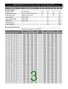
1.325 1.375 1.425 1.475 1.525 1.575 1.625 1.675 1.725 1.775 1.825 1.875 1.925 1.975 2.025 2.075
Load Capacitance (pF)
DAC Output Voltage Setting (V)
Figure 2: Gate(H) and Gate(L) Risetime vs. Load Capacitance.
Figure 5: Percent Output Error vs. DAC Output
Voltage Setting, VID4 = 1.
150
V
= 12V
= 25°C
125
100
75
50
25
0
CC
0.35
T
A
0.30
0.25
0.20
0.15
0.10
0
2000
4000
6000
8000
10000 12000 14000 16000
0.05
0
Load Capacitance (pF)
−0.05
−0.10
−0.15
−0.20
−0.25
V
= 12V
= 25°C
= 1
CC
Figure 3: DAC Output Voltage vs. Temperature,
DAC Code = 00001.
T
A
V
ID4
2.125 2.225 2.325 2.425 2.525 2.625 2.725 2.825 2.925 3.025 3.125 3.225 3.335 3.425 3.525
0.10
0.05
0
DAC Output Voltage Setting (V)
V
CC
= 12V
−0.05
−0.10
−0.15
0
20
40
60
80
100
120
Junction Temperature (°C)
Application Information
tains the DC portion of the output voltage, which allows
Theory Of Operation
the control circuit to drive the main switch to 0% or 100%
duty cycle as required.
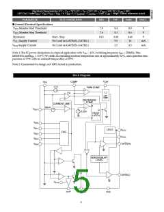
V2TM Control Method
The V2TM method of control uses a ramp signal that is gen-
erated by the ESR of the output capacitors. This ramp is
proportional to the AC current through the main inductor
and is offset by the value of the DC output voltage. This
control scheme inherently compensates for variation in
either line or load conditions, since the ramp signal is gen-
erated from the output voltage itself. This control scheme
differs from traditional techniques such as voltage mode,
which generates an artificial ramp, and current mode,
which generates a ramp from inductor current.
PWM
Comparator
–
GATE(H)
C
GATE(L)
+
Output
Voltage
Feedback
Ramp Signal
V
FB
Error
Amplifier
–
+
The V2TM control method is illustrated in Figure 6. The out-
put voltage is used to generate both the error signal and
the ramp signal. Since the ramp signal is simply the output
voltage, it is affected by any change in the output regard-
less of the origin of that change. The ramp signal also con-
COMP
E
Reference
Voltage
Error
Signal
TM
Figure 6: V2 Control Diagram
6

 CHERRY [ CHERRY SEMICONDUCTOR CORPORATION ]