Application Information: continued
Hysteresis of 300mV (typ) is provided for noise immunity.
The Error Amp Capacitor connected to the COMP pin is
charged by a 30µA current source. This capacitor must be
charged to 1.1V (typ) so that it exceeds the PWM compara-
tor’s offset before the V2TM PWM control loop permits
switching to occur.
When VCC1 has exceeded 8.4V and COMP has charged to
1.1V, the upper Gate driver (GATE(H)) is activated, turn-
ing on the upper FET. This causes current to flow through
the output inductor and into the output capacitors and
load according to the following equation:
T
I = (VIN – VOUT) ×
L
GATE(H) and the upper NFET remain on and inductor cur-
rent ramps up until the initial pulse is terminated by either
the PWM control loop or the overcurrent protection. This
initial surge of in-rush current minimizes startup time, but
avoids overstressing of the regulator’s power components.
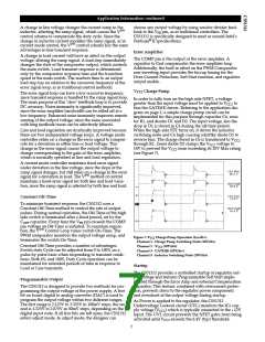
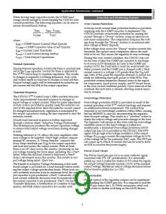
Figure 9: Normal Startup showing initial pulse followed by Soft Start
(5µs/div).
Channel 1 - VCC2 (10V/div)
Channel 2 – GATE(H) (10V/div)
The PWM comparator will terminate the initial pulse if the
regulator output exceeds the voltage on the COMP pin
plus the 1.1V PWM comparator offset prior to the drop
across the current sense resistor exceeding the current limit
threshold. In this case, the PWM control loop has achieved
regulation and the initial pulse is then followed by a con-
stant off time as programmed by the COFF capacitor. The
COMP capacitor will continue to slowly charge and the
regulator output voltage will follow it, less the 1.1V PWM
offset, until it achieves the voltage programmed by the
DAC’s VID input. The Error Amp will then source or sink
current to the COMP cap as required to maintain the cor-
rect regulator DC output voltage. Since the rate of increase
of the COMP pin voltage is typically set much slower than
the regulator’s slew capability, inrush current, output volt-
age, and duty cycle all gradually increase from zero. (See
Figures 8 and 9).
Channel 3 - Inductor Switching Node (10V/div)
Channel 4 - Regulator Output Voltage (2V/div)
If the voltage across the Current Sense resistor generates a
voltage difference between the VFB and VOUT pins that
exceeds the OVC Comparator Offset Voltage (86mV typi-
cal), the Fault latch is set. This causes the COMP pin to be
quickly discharged, turning off GATE(H) and the upper
NFET since the voltage on the COMP pin is now less than
the 1.1V PWM comparator offset. The Fault latch is reset
when the voltage on the COMP decreases below the
Discharge threshold voltage (0.25V typical). The COMP
capacitor will again begin to charge, and when it exceeds
the 1.1V PWM comparator offset, the regulator output will
Soft Start normally (see Figure 10).
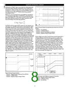
Figure 8: Normal Startup (5ms/div).
Channel 1 - Regulator Input Voltage and VCC1 (10V/div)
Channel 2 – COMP (2V/div)
Channel 4 - Regulator Output Voltage (1V/div)
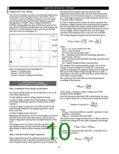
Figure 10: Startup with COMP pre-charged to 2V (2ms/div).
Channel 1 - Regulator Output Voltage (1V/div)
Channel 2 - COMP Pin (1V/div)
Channel 3 - VCC (10V/div)
8

 CHERRY [ CHERRY SEMICONDUCTOR CORPORATION ]