Application Information: continued
choose any output voltage by using resistor divider feed-
A change in line voltage changes the current ramp in the
TM
inductor, affecting the ramp signal, which causes the V2
control scheme to compensate the duty cycle. Since the
back to the VFB pin, as in traditional controllers. The
CS51312 is specifically designed to meet or exceed Intel’s
Pentium® II specifications.
change in inductor current modifies the ramp signal, as in
current mode control, the V2TM control scheme has the same
advantages in line transient response.
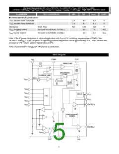
Error Amplifier
A change in load current will have an affect on the output
voltage, altering the ramp signal. A load step immediately
changes the state of the comparator output, which controls
the main switch. Load transient response is determined
only by the comparator response time and the transition
speed of the main switch. The reaction time to an output
load step has no relation to the crossover frequency of the
error signal loop, as in traditional control methods.
The error signal loop can have a low crossover frequency,
since transient response is handled by the ramp signal loop.
The main purpose of this ‘slow’ feedback loop is to provide
DC accuracy. Noise immunity is significantly improved,
since the error amplifier bandwidth can be rolled off at a
low frequency. Enhanced noise immunity improves remote
sensing of the output voltage, since the noise associated
with long feedback traces can be effectively filtered.
Line and load regulation are drastically improved because
there are two independent voltage loops. A voltage mode
controller relies on a change in the error signal to compen-
sate for a deviation in either line or load voltage. This
change in the error signal causes the output voltage to
change corresponding to the gain of the error amplifier,
which is normally specified as line and load regulation.
The COMP pin is the output of the error amplifier. A
capacitor to Gnd compensates the error amplifier loop.
Additionally, the built in offset on the PWM Comparator
non-inverting input provides the hiccup timing for the
Over-Current Protection, Soft Start function, and regulator
output enable.
VCC2 Charge Pump
In order to fully turn on the high side NFET, a voltage
greater than the input voltage must be applied to VCC2 to
bias the GATE(H) driver. Referring to the application dia-
gram on page 1; a simple charge pump circuit can be
implemented for this purpose through capacitor C6, resis-
tor R1, and diodes D1 and D2. The input voltage, less the
drop in D1 is stored in C6 during the off-time period.
When the high-side FET turns on, it drives the inductor
switching node and C6 high causing schottky diode D1 to
reverse bias. The charge stored in C6 is transferred to VCC2
through R1. Zener diode D2 clamps the VCC2 voltage to
18V to prevent the VCC2 from exceeding its 20V Max rating
(see Figure 7).
A current mode controller maintains fixed error signal
under deviation in the line voltage, since the slope of the
ramp signal changes, but still relies on a change in the error
signal for a deviation in load. The V2TM method of control
maintains a fixed error signal for both line and load varia-
tion, since the ramp signal is affected by both line and load.
Constant Off-Time
To minimize transient response, the CS51312 uses a
Constant Off-Time method to control the rate of output
pulses. During normal operation, the Off-Time of the high
side switch is terminated after a fixed period, set by the
COFF capacitor. Every time the VFB pin exceeds the COMP
pin voltage an Off-Time is initiated. To maintain regula-
tion, the V2TM Control Loop varies switch On-Time. The
PWM comparator monitors the output voltage ramp, and
terminates the switch On-Time.
Constant Off-Time provides a number of advantages.
Switch duty Cycle can be adjusted from 0 to 100% on a
pulse-by pulse basis when responding to transient condi-
tions. Both 0% and 100% Duty Cycle operation can be
maintained for extended periods of time in response to
Load or Line transients.
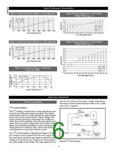
Figure 7: VCC2 Charge Pump Operation (1µs/div).
Channel 1 - Charge Pump Switching Node (10V/div)
Channel 2 - VCC2 (10V/div)
Channel 3 - GATE(H) (10V/div)
Channel 4 - Inductor Switching Node (10V/div)
Startup
The CS51312 provides a controlled startup of regulator out-
put voltage and features Programmable Soft Start imple-
mented through the Error Amp and external Compensation
Capacitor. This feature, combined with overcurrent protec-
tion, prevents stress to the regulator power components
and overshoot of the output voltage during startup.
Programmable Output
The CS51312 is designed to provide two methods for pro-
gramming the output voltage of the power supply. A five
bit on board digital to analog converter (DAC) is used to
program the output voltage within two different ranges.
The first range is 2.125V to 3.525V in 100mV steps, the sec-
ond is 1.325V to 2.075V in 50mV steps, depending on the
digital input code. If all five bits are left open, the CS51312
enters adjust mode. In adjust mode, the designer can
As Power is applied to the regulator, the CS51312
Undervoltage Lockout circuit (UVL) monitors the ICs sup-
ply voltage (VCC1) which is typically connected to the +12V
input. The UVL circuit prevents the NFET gates from being
activated until VCC1 exceeds the 8.4V (typ) threshold.
7

 CHERRY [ CHERRY SEMICONDUCTOR CORPORATION ]