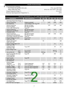
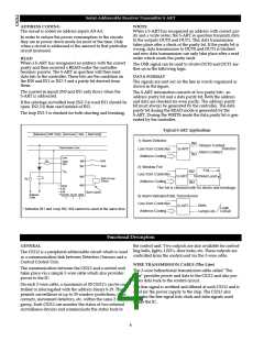
Functional Description: continued
INPUTS:
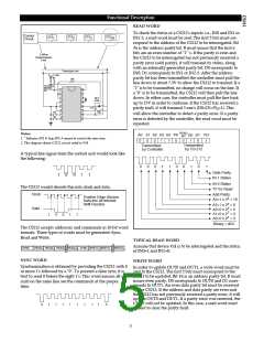
WRITE
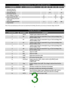
1. Address inputs: Pin#'s 2,3,4,5,6.
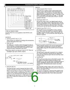
A0 A1 A2 A3 A4 PA BIT D0 D1 PD
The CS212 has 5 address inputs which decide what
address code it will respond to. Their thresholds are
approximately 1/2 VDD and draw less than 20µA. The
inputs should be grounded for Logic "0" and tied to VDD
(PIN 12) through a 10K resistor for Logic "1". The resis-
tor is necessary for non-destruction of the IC with 28V
applied to the line.
0 1 0 0 0 1 1 1 0 1
0 1 0 0 0 1 1 1 0 1
Data Parity
OUT 1
OUT 0
2. Data Inputs: Pin#'s 7,8.
"1" for Write
Add Parity
IN0 and IN1 (Pins 8 and 7) are digital inputs and are
similar to the address inputs in that they have a thresh-
old of approximately 1/2 VDD. When the CS212 is unad-
dressed, these inputs draw less than 20µA. When the
circuit powers up, IN0 and IN1 typically source 400µA.
A4=0 x 24 = 0
A3=0 x 23 = 0
A2=0 x 22 = 0
A1=1 x 21 = 2
A0=0 x 20 = 0
3. Detector Loop: Pin #'s 13, 14.
Binary = #2
IN2 and IN3 can be used together to form a detector
loop. When used, the outputs are connected together
through a window foil and a diode. These inputs will
generate a logic Ò1Ó at D1 on the line when the pins are
shorted or opened.
TYPICAL WRITE WORD:
Assume CS212 #2 is to be updated so that OUT0=1 and
OUT1=0.
OUTPUTS
1 When IN 1=1
IN 1
1. OUT0 and OUT1: Pin #'s 1, 16:
T0 D, Online
Durning Read
IN 2
IN 3
These outputs are updated according to the information
present during the write word.
Loop Status
DET.
1 When Loop
is Open or Shorted
2. DSR: Pin #15:
The DSR pin is a monitor of the clock signal for the on-
chip D flip flops, corresponding to OUT0 and OUT1. It
can be used to strobe data from OUT0 and OUT1 into
external circuitry connected to the CS212.
When using IN2 and IN3, IN1 must be terminated to
VDD through the 10K Resistor used for the address
inputs. When using IN1, IN2 and IN3 must be shorted
or opened.
These three outputs can sink up to 1mA at 1.2V. They are
Darlington type open collector outputs.
4. Line Input: Pin #9
The line input is internally connected to two compara-
tors. These comparators separate the line signal into
clock and data. The line input will draw less than 16µA
of input current.
OUT 0, OUT 1, DSR
5. VDD: Pin #12
LINE
DSR
The VDD Pin provides power to the CS212 circuitry. The
line signal is externally rectified and filtered, then
applied to VDD. The VDD pin draws varying amounts of
current, depending upon the state of the CS212. (See
specification). The unaddressed current is less than
0.8mA.
The Edge is Present
When OUT 0 & OUT 1 are Updated.
The operating voltage range is 10V to 18V on Pin 12 of
the IC. This wide range is necessary because of losses in
3. Data Out: Pin #11:
The Data Out pin is used to transmit the status of IN0
and IN1 to the line. For Data=1, the line driver is off. For
Data=0, the line driver is turned on. This output is a sat-
urated switch capable of sinking 10mA DC at .4V and
50mA at 1V on a transient basis. The 50mA is needed to
discharge the line capacitance. A 150½ resistor from the
line to Pin 11 limits the current into Pin 11 when the line
driver is on.
the line and ripple on VDD
.
The circuit is designed to withstand 28V applied to the
line. This is to prevent the destruction of the IC and its
external components if the 2-wire cable is miswired.
6

 CHERRY [ CHERRY SEMICONDUCTOR CORPORATION ]