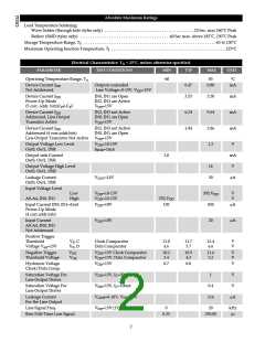
Electrical Characteristics: TA = 25¡C, unless otherwise specified.
PARAMETER
TEST CONDITIONS
MIN
TYP
MAX
UNIT
Turn-On Time For
Line Output Driver
1.0
µs
Turn-Off Time For
Line Output Driver
1.0
µs
Line Voltage VL (Note 1)
Loop Current IN2, IN3
0
0.1
1
28
0.5
5
V
mA
k½
Alarm Condition IN2-IN3
Loop Open
Alarm Condition IN2-IN3
Loop Shorted
5
30
k½
Note 1: The circuit shall function in the correct way only between 0 and 18VDC. Data driver must not turn on when line voltage is above 18V.
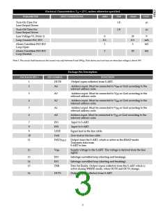
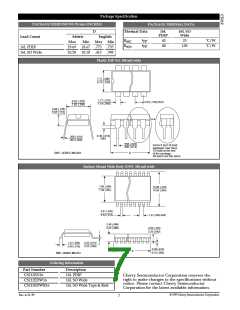
Package Pin Description
PACKAGE PIN #
PIN SYMBOL
OUT0
FUNCTION
1
2
Output (open collector) from S-ART.
A4
Address input. Must be connected to VDD or Gnd according to the
relevant address code.
3
4
5
6
A3
A2
A1
A0
Address input. Must be connected to VDD or Gnd according to the
relevant address code.
Address input. Must be connected to VDD or Gnd according to the
relevant address code.
Address input. Must be connected to VDD or Gnd according to the
relevant address code.
Address input. Must be connected to VDD or Gnd according to the
relevant address code.
7
8
IN1
Input to S-ART.
IN0
Input to S-ART.
9
LINE
Gnd
Signal lead in the line cable.
Zero lead in the line cable.
10
11
DATAOUT
Output from the S-ART, which is active in the READ-mode.
Transmits data from
S-ART to line.
12
VDD
Supply voltage to the S-ART. The voltage is derived from the line
signal.
13
14
15
IN3
IN2
DSR
Sabotage surveilled loop (shorting and breaking).
Sabotage surveilled loop (shorting and breaking).
Data Set Ready. Output (open collector) from the S-ART which is
active during WRITE-mode, when OUT0 and OUT1 change.
16
OUT1
Output (open collector) from S-ART.
3

 CHERRY [ CHERRY SEMICONDUCTOR CORPORATION ]