VS1005g Datasheet
4
CHARACTERISTICS & SPECIFICATIONS
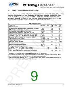
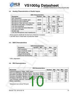
4.3 Analog Characteristics of Audio Outputs
Unless otherwise noted: AVDD=3.6V, CVDD=1.8V, IOVDD=2.8V, Vref=1.6V, TA=+25◦C, XTALI=12 MHz,
Internal Clock Multiplier 3.0×. DAC tested with full-scale output sinewave, measurement band-
width 20..20000 Hz, analog output load: LEFT to CBUF 30 Ω, RIGHT to CBUF 30 Ω. Micro-
phone test amplitude 50 mVpp, f=1 kHz, Line input test amplitude 2.2 Vpp, f=1 kHz. FM test
signal input level -70 dBm, deviation 75 kHz, pre-emphasis 50 us, f=1 kHz.
DAC Characteristics
Parameter
Symbol Min Typ Max Unit
DAC Resolution
24
100
92
bits
dB
dB
dB
%
%
dB
Dynamic range (DAC unmuted, A-weighted, min gain)
S/N ratio (full scale signal, no load)
S/N ratio (full scale signal, 30 ohm load)
Total harmonic distortion, -3dB level, no load
Total harmonic distortion, -3dB level, 30 ohm load
Crosstalk (L/R to R/L), 30 ohm load, without CBUF 1
Crosstalk (L/R to R/L), 30 ohm load, with CBUF
Gain mismatch (L/R to R/L)
Frequency response
Full scale output voltage
Deviation from linear phase
Analog output load resistance
IDR
SNR
SNRL
THD
THDL
XTALK1
XTALK2
GERR
AERR
LEVEL
PH
90
0.01
0.05
-75
-54
dB
-0.5
-0.05
0.5 dB
0.05 dB
1.0
0
V◦ rms
5
AOLR
AOLC
302
Ω
Analog output load capacitance
1003 pF
DC level, Vref =1.2V (CBUF, LEFT, RIGHT)
DC level, Vref =1.6V (CBUF, LEFT, RIGHT)
CBUF disconnect current (short-circuit protection)
1.1
1.5
1.3
1.7
V
V
130 200 mA
1
2
Loaded from Left/Right pin to analog ground via 100 µF capacitors.
AOLR may be lower than Typical, but distortion performance may be compromised. Also,
there is a maximum current that the internal regulators can provide.
3
CBUF must have external 10 Ω + 47 nF load, LEFT and RIGHT must have external 20 Ω +
10 nF load for optimum stability and ESD tolerance.
Version: 0.2, 2012-03-16
9

 ETC [ ETC ]