VS1005g Datasheet
4
CHARACTERISTICS & SPECIFICATIONS
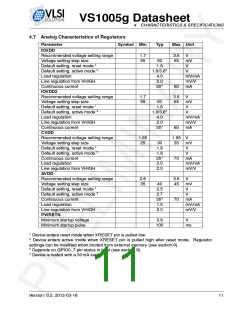
4.7 Analog Characteristics of Regulators
Parameter
Symbol Min
Typ
Max Unit
IOVDD
Recommended voltage setting range
Voltage setting step size
Default setting, reset mode 1
Default setting, active mode 2
Load regulation
1.7
55
3.6
65
V
mV
V
60
1.8
1.8/3.63
4.0
V
mV/mA
mV/V
mA
Line regulation from VHIGH
Continuous current
2.0
304
60
IOVDD2
Recommended voltage setting range
Voltage setting step size
Default setting, reset mode 1
Default setting, active mode 2
Load regulation
1.7
55
3.6
65
V
mV
V
60
1.8
1.8/3.63
4.0
V
mV/mA
mV/V
mA
Line regulation from VHIGH
Continuous current
2.0
304
60
CVDD
Recommended voltage setting range
Voltage setting step size
Default setting, reset mode 1
Default setting, active mode 2
Continuous current
Load regulation
Line regulation from VHIGH
AVDD
1.65
25
1.95
35
V
mV
V
30
1.8
1.8
254
2.0
2.0
V
70
mA
mV/mA
mV/V
Recommended voltage setting range
Voltage setting step size
Default setting, reset mode 1
Default setting, active mode 2
Continuous current
Load regulation
Line regulation from VHIGH
PWRBTN
2.6
35
3.6
45
V
mV
V
40
2.5
2.7
304
1.5
2.0
V
70
mA
mV/mA
mV/V
Minimum startup voltage
Minimum startup pulse
0.9
100
V
ms
1
2
Device enters reset mode when XRESET pin is pulled low.
Device enters active mode when XRESET pin is pulled high after reset mode. Regulator
settings can be modified when booted from external memory (see section 9).
3
Depends on GPIO0_7 pin status in boot (see section 9).
Device is tested with a 30 mA load.
4
Version: 0.2, 2012-03-16
11

 ETC [ ETC ]