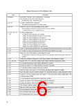
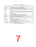
Major Revisions in This Edition (1/2)
Page
Throughout
Description
µPD78070A, 78070AY: Under development → Developed
The following products were added (planned)
µPD78070AGC-8EU, 78070AYGC-8EU
p. 40, 50
p. 66, 82
1.5 and 2.5 78K/0 Series Expansion
The contents were updated to the latest version
Tables 3-1. and 4-1. Pin Input/Output Circuit Types
Recommended connection of unused P07/XT1 pin was modified
Connect to VDD or VSS → Connect to VDD
p. 119 to 123, 127,
130
6.2 Port Configuration
The following block diagrams were modified
Figure 6-5. Block Diagram of P20, P21, P23 to P26
Figure 6-6. Block Diagram of P22 and P27
Figure 6-7. Block Diagram of P20, P21, P23 to P26
Figure 6-8. Block Diagram of P22 and P27
Figure 6-9. Block Diagram of P30 to P37
Figure 6-13. Block Diagram of P71 and P72
Figure 6-16. Block Diagram of P100 and P101
p. 143
p. 155
p. 166
Table 7-2. Relationship between CPU Clock and Minimum Instruction Execution Time was added
8.1 Outline of Timers Incorporated into µPD78070A and 78070AY was added
Figure 8-4. 16-bit Timer Mode Control Register Format
The generation conditions of interrupt requests in the operation mode and the clear mode were
modified
p. 168
Caution was modified in Figure 8-6. 16-bit Timer Output Control Register Format
Figures 9-10., 9-13., and 10-13. Square-wave Output Operation Timing were added
12.3 (2) Watchdog timer mode register (WDTM) was modified
p. 215, 220, 237
p. 256
p. 294
Caution was added in 17.1 Serial Interface Channel 0 Functions
p. 298
17.2 (2) Slave address register (SVA) was modified
p. 302
Note and Caution were added in 17.3 (2) Serial operating mode register 0 (CSIM0)
Note of the BSYE flag was modified in Figure 17-5. Serial Bus Interface Control Register Format
p. 305
p. 315
Cautions on the bus change timing were added in 17.4.3 (2) (a) Bus release signal (REL), (b)
Command signal (CMD)
p. 331
p. 346
p. 350
p. 350
p. 354
p. 380
p. 390
p. 391
17.4.3 (6) Address match detection method was modified
Caution was added in 18.1 Serial Interface Channel 0 Functions
Caution was added in 18.2 (1) Serial I/O shift register 0 (SIO0)
18.2 (2) Slave address register (SVA) was modified
Note and Caution were added in 18.3 (2) Serial operating mode register 0 (CSIM0)
18.4.4 (6) Address match detection method was modified
18.4.5 (3) Slave wait release (slave reception) was added
18.4.6 Restrictions in I2C bus mode was added
6

 ETC [ ETC ]